This thread has been locked.

If you have a related question, please click the "Ask a related question" button in the top right corner. The newly created question will be automatically linked to this question.

ADS8588SEVM-PDK: Using the ADS8588SEVM as a stand-alone board without PHI board

Part Number: ADS8588SEVM-PDK
Other Parts Discussed in Thread: ADS8588S

Dear Technical Support Team,

I'd like to use the ADS8588SEVM as a stand-alone board without PHI board.

Q1-1

Is it possible to supply 2.5V to the 50-pin DVDD of the J9 connector from FPGA board?
Since the IO on the connected FPGA board side is 2.5V, I would like to use the Digital Output on the ADS8588S side as LVCMOS2.5V.

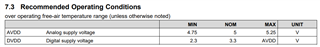
DC specifications of ADS8588S says that range of DVDD shows from 2.3V (min) to AVDD, so 2.5V seems to be no problem.

But if it is not intended to be used as LVCMOS 2.5V, is it better to avoid it?

Q1-2

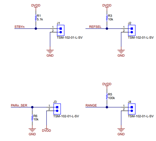
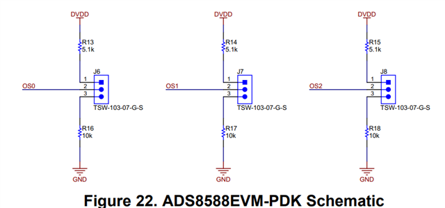
I'd like to know if other restrictions(Such as pullup/GND for STBYn /  REFSEL / PARn_SER / RANGE / OS0/1/2 ) on  ADS8588SEVM  with DVDD=2.5V.

Q2

If it can be used with DVDD=2.5V, are the following VOL/VOH specifications of Digital IO correct?

VIH = 1.75V~2.8V
VIL = -0.3V~0.75V
VOH = 2.0V~2.5V
VOL = 0V~0.5V

Q3

Is it okay if pins 56, 58, and 59 of the J9 connector are floating?

I think the EEPROM contains information to inform the PHI board that the ADS8588S is installed on ADS8588SEVM , but I will not use PHI and use FPGA board.

Q4

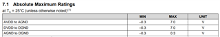
Datasheet  "10 Power Supply Recommendations" shows following and it seems no sequencing between AVDD and DVDD.

----

There are no specific requirements with regard to the power-supply sequencing of the device. However, issue a reset after the supplies are powered and are stable to ensure the device is properly configured.

----

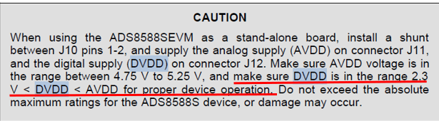
ADS8588EVM-PDK shows following.

Dose Red lined "make sure DVDD is in the range 2.3 V < DVDD < AVDD for proper device operation. " mean sequencing (First AVDD and Second DVDD) or no sequencing(Just a Voltage level)?

In my case, DVDD=2.5V are from FPGA through J9. 

Is it OK in either order, DVDD => AVDD or AVDD => DVDD, and after the power supply is stable, is it proper device operation to set the initial ADC settings from FPGA after reset?

Best Regards,

ttd

  • Hi ttd,

    I will look into the details and get it back to you tomorrow.

    Regards,

    Dale

  • Hi ttd,

    Please see my answers below:

    1-1. You can do that, but the specifications shown in the data sheet were charactizated under AVDD=5V and DVDD=3V. You may see a slightly different performance with your power supply.

    1-2. No other restrictions.

    2. These should be right.

    3. Yes, you can leave these pins floating as you will not use PHI card and the EVM GUI software, these three pins are only used for EEPROM which is used for the EVM GUI software.

    4. I suggest you to follow the guideline in the datasheet.

    Regards,

    Dale

  • Hi Dale,

    Thank you for your reply.

    When Reset is issued, then ADC start to initialized with dedicated pin such as pullup/GND for STBYn /  REFSEL / PARn_SER / RANGE / OS0/1/2 ?

    Also I'd like to confirm the following the detail of caution.

    Make sure AVDD voltage is in the range between 4.75 V to 5.25 V, and make sure DVDD is in the range 2.3 V < DVDD < AVDD for proper device operation.

    ⇒Does it mean the range for Recommended Operating Conditions?

       Since there are no regulations regarding the power supply sequence, I understand that even if the above relationship occurs for a moment, the device will not be damaged.
    For example, am I correct in my understanding that the device will not be damaged if only AVDD(5V) or only DVDD(2.5V) is turned on, and that it will operate correctly if set to 2.3V < DVDD (2.5V) < AVDD (5V)?

    Do not exceed the absolute maximum ratings for the ADS8588S device, or damage may occur.

    ⇒Dose it mean following absolute max?

        it means that AVDD and DVDD must not exceed 7V.

    Best Regards,

    ttd

  • Hi ttd,

    1. Those pins you mentioned are input pins. You have to provide an input (high or low) for those pins. The RESET signal on the RESET pin will reset all digital circuitry in the device.

    2. Yes, these are recommended operating conditions in the table 7.3 you are showing.

    3. There is no relationship between AVDD and DVDD, they are used for different circuits. The ADC will not be damaged as long as the specifications in the table of Absolute Maximum Ratings (AMR) are not violated. For example, the safety can not be guaranteed if you apply a signal to the ADC's digital input before DVDD is turned, this condition violates the specification in the AMR table.

    4. Yes, that is the Absolute Maximum Ratings table, see my explanation above. The AMR table can guarantee the safety for the ADC, the recommended operating conditions can achieve the performance specified in the datasheet.

    Regards,

    Dale