Part Number: DAC3283EVM
Other Parts Discussed in Thread: DAC3283, CDCE62005
we have Interfaced the DAC3283 with the Iwave systems FPGA. We are able to configure the CDCE with following frequencies:
DAC clk : 614 MHz
FIFO OSTR clk : 19.2 Mhz
FPGA clk : 76.8 Mhz
Interpolation : 4x
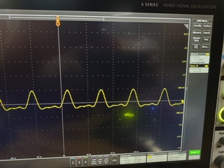
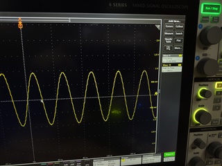
We generate a square signal using FPGA clk inside FPGA and sent it to DAC.
Data clk : 307.2 MHz
Frame clk: 19.2 Mhz
Frequency of square signal :38.4 Mhz
We are trying to see DAC output at J3 connector after doing the necessary changes mentioned in section 4.1 of DAC3283 User Guide.
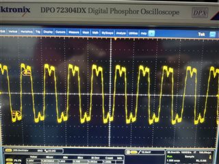
We have checked using oscilloscope that all above mentioned clock and data are reaching to DAC pins, But there is no output from J3. IOUT pins on DAC IC always shows constant 3.3V, even if data from FPGA is not present.
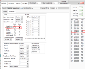
Configuration file is also attached, which is used to configure DAC3283 and CDCE62005.
Texas Instruments Inc.
DAC32x2 EVM Register Configuration

DAC32x2 Registers
Address	Data
00		30
01		31
02		00
03		10
04		FF
05		30
06		00
07		20
08		F5
09		7A
0A		B6
0B		EA
0C		45
0D		1A
0E		16
0F		AA
10		C6
11		24
12		02
13		00
14		00
15		00
16		00
17		00
18		80
19		00
1A		00
1B		00
1C		00
1D		00
1E		24
1F		12
20		00
21		00

CDCE62005 Registers
Freq:19.200000MHz
Address	Data
00		01040300
01		81400321
02		811C0302
03		81040303
04		01040304
05		381C0A85
06		04BE1F26
07		3D98F7F7
08		20001808
<Cluster>
<Name></Name>
<NumElts>9</NumElts>
<Cluster>
<Name>Freq Calculations</Name>
<NumElts>6</NumElts>
<EXT>
<Name>VCO Freq Actual[MHz]</Name>
<Val>2408.00000</Val>
</EXT>
<EXT>
<Name>RF Freq Actual[MHz]</Name>
<Val>2408.00000</Val>
</EXT>
<EXT>
<Name>PFD Freq Actual[MHz]</Name>
<Val>0.80000</Val>
</EXT>
<DBL>
<Name>RF Stepsize [MHz]</Name>
<Val>0.80000</Val>
</DBL>
<DBL>
<Name>Fraction [KHz]</Name>
<Val>0.00000</Val>
</DBL>
<DBL>
<Name>CAL_CLK_FREQ [MHz]</Name>
<Val>5.00000E-2</Val>
</DBL>
</Cluster>
<Cluster>
<Name>Freq Targets</Name>
<NumElts>5</NumElts>
<DBL>
<Name>Ref Freq[MHz]</Name>
<Val>76.80000</Val>
</DBL>
<EXT>
<Name>RF Target [MHz]</Name>
<Val>2408.00000</Val>
</EXT>
<DBL>
<Name>INT Step (MHz)</Name>
<Val>0.80000</Val>
</DBL>
<I8>
<Name>Int/Frac Select</Name>
<Val>0</Val>
</I8>
<Boolean>
<Name>stop</Name>
<Val>1</Val>
</Boolean>
</Cluster>
<Cluster>
<Name>Reg1</Name>
<NumElts>9</NumElts>
<I8>
<Name>ADDR</Name>
<Val>9</Val>
</I8>
<I16>
<Name>RDIV</Name>
<Val>96</Val>
</I16>
<I8>
<Name>RSV</Name>
<Val>0</Val>
</I8>
<I8>
<Name>REF_INV</Name>
<Val>0</Val>
</I8>
<I8>
<Name>NEG_VCO</Name>
<Val>1</Val>
</I8>
<I8>
<Name>ICP</Name>
<Val>0</Val>
</I8>
<I8>
<Name>ICPDOUBLE</Name>
<Val>0</Val>
</I8>
<I16>
<Name>CAL_CLK_SEL</Name>
<Val>12</Val>
</I16>
<I8>
<Name>RSV 2</Name>
<Val>0</Val>
</I8>
</Cluster>
<Cluster>
<Name>Reg2</Name>
<NumElts>9</NumElts>
<I8>
<Name>ADDR</Name>
<Val>10</Val>
</I8>
<U16>
<Name>NINT</Name>
<Val>3010</Val>
</U16>
<I8>
<Name>PLL_DIV_SEL</Name>
<Val>0</Val>
</I8>
<I8>
<Name>PRSC_SEL</Name>
<Val>1</Val>
</I8>
<I8>
<Name>RSV</Name>
<Val>0</Val>
</I8>
<I8>
<Name>VCO_SEL</Name>
<Val>2</Val>
</I8>
<I8>
<Name>VCOSEL_MODE</Name>
<Val>0</Val>
</I8>
<I8>
<Name>CAL_ACC</Name>
<Val>0</Val>
</I8>
<I8>
<Name>EN_CAL</Name>
<Val>0</Val>
</I8>
</Cluster>
<Cluster>
<Name>Reg3</Name>
<NumElts>3</NumElts>
<I8>
<Name>ADDR</Name>
<Val>11</Val>
</I8>
<U32>
<Name>NFRAC</Name>
<Val>0</Val>
</U32>
<I8>
<Name>RSV</Name>
<Val>0</Val>
</I8>
</Cluster>
<Cluster>
<Name>Reg4</Name>
<NumElts>25</NumElts>
<I8>
<Name>ADDR</Name>
<Val>12</Val>
</I8>
<I8>
<Name>PWD_PLL</Name>
<Val>0</Val>
</I8>
<I8>
<Name>PWD_CP</Name>
<Val>0</Val>
</I8>
<I8>
<Name>PWD_VCO</Name>
<Val>0</Val>
</I8>
<I8>
<Name>PWD_VCOMUX</Name>
<Val>0</Val>
</I8>
<I8>
<Name>PWD_DIV124</Name>
<Val>0</Val>
</I8>
<I8>
<Name>PWD_PRESC</Name>
<Val>0</Val>
</I8>
<I8>
<Name>PWD_RESYNC</Name>
<Val>0</Val>
</I8>
<I8>
<Name>PWD_OUT_BUFF</Name>
<Val>1</Val>
</I8>
<I8>
<Name>PWD_LO_DIV</Name>
<Val>1</Val>
</I8>
<I8>
<Name>PWD_TX_DIV</Name>
<Val>0</Val>
</I8>
<I8>
<Name>PWD_BB_VCM</Name>
<Val>0</Val>
</I8>
<I8>
<Name>PWD_DC_OFF</Name>
<Val>0</Val>
</I8>
<I8>
<Name>EN_EXTVCO</Name>
<Val>0</Val>
</I8>
<I8>
<Name>EN_ISOURCE</Name>
<Val>0</Val>
</I8>
<I8>
<Name>LD_ANA_PREC0</Name>
<Val>0</Val>
</I8>
<I8>
<Name>LD_ANA_PREC1</Name>
<Val>0</Val>
</I8>
<I8>
<Name>CP_TRISTATE</Name>
<Val>0</Val>
</I8>
<I8>
<Name>SPEEDUP</Name>
<Val>0</Val>
</I8>
<I8>
<Name>LD_DIG_PREC</Name>
<Val>0</Val>
</I8>
<I8>
<Name>EN_DITH</Name>
<Val>1</Val>
</I8>
<I8>
<Name>MOD_ORD</Name>
<Val>2</Val>
</I8>
<I8>
<Name>DITH_SEL</Name>
<Val>0</Val>
</I8>
<I8>
<Name>DEL_SD_CLK</Name>
<Val>2</Val>
</I8>
<I8>
<Name>EN_FRAC</Name>
<Val>0</Val>
</I8>
</Cluster>
<Cluster>
<Name>Reg5</Name>
<NumElts>14</NumElts>
<I8>
<Name>ADDR</Name>
<Val>13</Val>
</I8>
<I8>
<Name>VCOBIAS_RTRIM</Name>
<Val>4</Val>
</I8>
<I8>
<Name>PLLBIAS_RTRIM</Name>
<Val>2</Val>
</I8>
<I8>
<Name>VCO_BIAS</Name>
<Val>8</Val>
</I8>
<I8>
<Name>VCOBUF_BIAS</Name>
<Val>2</Val>
</I8>
<I8>
<Name>VCOMUX_BIAS</Name>
<Val>3</Val>
</I8>
<I8>
<Name>BUFOUT_BIAS</Name>
<Val>0</Val>
</I8>
<I8>
<Name>RSV</Name>
<Val>0</Val>
</I8>
<I8>
<Name>VCO_CAL_IB</Name>
<Val>0</Val>
</I8>
<I8>
<Name>VCO_CAL_REF</Name>
<Val>2</Val>
</I8>
<I8>
<Name>VCO_AMPL_CTRL</Name>
<Val>3</Val>
</I8>
<I8>
<Name>VCO_VB_CTRL</Name>
<Val>0</Val>
</I8>
<I8>
<Name>VCO_MUX_GAIN</Name>
<Val>0</Val>
</I8>
<I8>
<Name>EN_LD_ISOURCE</Name>
<Val>0</Val>
</I8>
</Cluster>
<Cluster>
<Name>Reg6</Name>
<NumElts>8</NumElts>
<I8>
<Name>ADDR</Name>
<Val>14</Val>
</I8>
<I16>
<Name>IOFF</Name>
<Val>128</Val>
</I16>
<I16>
<Name>QOFF</Name>
<Val>128</Val>
</I16>
<I8>
<Name>VREF_SEL</Name>
<Val>4</Val>
</I8>
<I8>
<Name>TX_DIV_SEL</Name>
<Val>0</Val>
</I8>
<I8>
<Name>LO_DIV_SEL</Name>
<Val>0</Val>
</I8>
<I8>
<Name>TX_DIV_BIAS</Name>
<Val>1</Val>
</I8>
<I8>
<Name>LO_DIV_BIAS</Name>
<Val>2</Val>
</I8>
</Cluster>
<Cluster>
<Name>Reg7</Name>
<NumElts>14</NumElts>
<I8>
<Name>ADDR</Name>
<Val>15</Val>
</I8>
<I8>
<Name>RSV</Name>
<Val>0</Val>
</I8>
<I16>
<Name>VCO_TRIM</Name>
<Val>32</Val>
</I16>
<I8>
<Name>RSV 2</Name>
<Val>0</Val>
</I8>
<I8>
<Name>VCO_TESTMODE</Name>
<Val>0</Val>
</I8>
<I8>
<Name>CAL_BYPASS</Name>
<Val>0</Val>
</I8>
<I8>
<Name>MUX_CTRL</Name>
<Val>1</Val>
</I8>
<I8>
<Name>ISOURCE_SINK</Name>
<Val>0</Val>
</I8>
<I8>
<Name>ISOURCE_TRIM</Name>
<Val>4</Val>
</I8>
<I8>
<Name>PD_TC</Name>
<Val>0</Val>
</I8>
<I8>
<Name>IB_VCM_SEL</Name>
<Val>0</Val>
</I8>
<I8>
<Name>MIXLO_VCM</Name>
<Val>4</Val>
</I8>
<I8>
<Name>DCOFFSET_I</Name>
<Val>2</Val>
</I8>
<I8>
<Name>VCO_TRIM_SEL</Name>
<Val>1</Val>
</I8>
</Cluster>
</Cluster>