This thread has been locked.

If you have a related question, please click the "Ask a related question" button in the top right corner. The newly created question will be automatically linked to this question.

ADC32RF45: Our custom board(ADC32RF45 modified) doesn't communicate with TWS14J57EVM

Part Number: ADC32RF45
Other Parts Discussed in Thread: TSW14J57EVM, LMK04828, LMX2592, , LMH6401, LMH5401, LMX2582

Hi,

We has some problems that our board doesn't communicate with TWS14J57EVM using HSDC Pro.

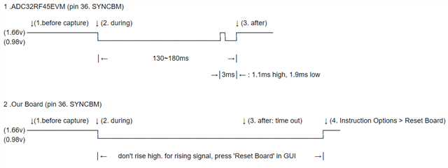
When I clicked the capture button,I observed a timeout message. The SYNC signal goes low and doesn't rise again.

Executing the "reset board" command in the GUI restores the SYNC signal to a high state. 

However, a timeout consistently occurs when clicking the capture button.

We made a custom board based on ADC32RF45EVM to measure high speed photo detector's signal.

Since we don't have an FPGA development environments and are currently using the TSW14J57EVM as is, we've decided to proceed with creating the custom board separately.

Our board included a micro controller(STM32F103) to Initialize ADC32RF45, LMK04828 and LMX2592 using SPI, and embedded LMH6401, LMH5401 for signal conditioning.

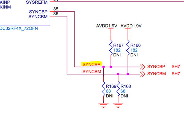
The wiring lengths for connections between chips or connect(FMC) changed by ADC32RF45EVM during the PCB board design.

I made efforts to equalize the lengths of the differential lines, considering the sensitivity of the JESD204B standard to timing issues.

We checked the clocks going to each chip since communication wasn't established. I confirmed that the clock frequencies match those of the ADC32RF45EVM.

However, due to the limited bandwidth of the our oscilloscope, precise measurement of signal timing between them was not possible.

We are currently suspecting the clock timing and data lane timing between boards.

In particular, we suspect that the shortened length of the data lanes compared to the reference EVM board may be causing issues.

We are curious whether this suspicion is valid and if there are other aspects we should investigate.

Your advice would be greatly appreciated. 

Thank you.

  • Hi Sanghyun,

    The shorter traces will not impact the link coming up as long as within each pair the traces are matched. Is the LED D3 blinking on the TSW14J57EVM? If not, I suspect the reference frequency to the FPGA is incorrect. When you enter the sampling rate into ADC Output Data Rate field, a informational message should appear and say the required reference clock frequency. Ensure this matches. HSDC Pro on every capture re-initializes the JESD link. If SYNC is toggled low when you press capture but does not rise again, then the ADC is not sending K28.5 characters or the FPGA is not receiving them. Physical trace lengths of the data lanes should not matter here as CGS occurs before ILAS phase. The issue of vastly different trace lengths will impact ILAS, not CGS. ILAS occurs after the FPGA receives 4 K28.5 symbols on each lane. This issue is often referred to as "stuck in CGS phase". Something to try is place the ADC into repeating K28.5 test pattern mode using register field: LINK LAYER TESTMODE

    Regards, Chase

  • Hi Chase

    Thanks for your reply.

    I describe our condition. When stm32 finished initialization of ADC in the board, the LED D3(RX SYNC) is blinking at a 9 second interval.
    We use internal CLK at 2949.12M using LMK04828 & LMX2592 and set registers using LMX_2949p12M.cfg, LMK_ADC32RF45_bypass_2949Msps.cfg, ADC32RF45_8224.cfg files in ADC32RFxx EVM GUI folder.
    For repeating K28.5 test pattern mode, I modified stm32's ADC init code. Set 0x60 at 0x690003 (JESD DIG CH A, B) and unset (0x00) to 0x690003 in main loop with 100ms interval.
    However, the timeout in HSDC GUI consistently occurs. TX SYNC(LED D1) is high.

    If I've made a mistake in the settings, please provide more specific guidance on how to resolve the issue.

    Thanks

  • Hi Sanghyun,

    Are you able to probe the SYNCBP/M net of the EVM at these resistors below at the following stages:

    1. before pressing the capture button
    2. during press of the capture button
    3. after capture button is pressed.

    Ensure bits 7 and 6 of register 0x002 of JESD digital page are both set to 0 to use hardware SYNCb.

    Regards, Chase

  • I was probe SYNCBM(36) EVM and our board.

    I couldn't upload images in my company, so I am drawing the signals using ASCII characters. sorry..

    Regards

  • probing image upload! 

  • Hi Sanghyun,

    Sorry for the delay. Thanks for sharing this. When you program the ADC32RF45EVM, can you make note of the pulsing LED on the TSW14J57EVM. When the custom board is used, is the light pulsing at the same rate?

    Thanks, Chase

  • The lights are pulsing at the same rate. (D2, D3)

    We were initialized our board 3 ini files in ADC32RFxx EVM GUI folder. (2949.12M, Bypass, 14bit)

    EVM setting in Quick Setup tab at ADC32RFxx EVM GUI 

    1. Nyquist zone: 2st Nyquist

    2. Clk source: LMX2582 to ADC

    3. Internal Clk Freq: 2949.12Msps

    4. ADC mode: Bypass

    5. Resolution: 14bit

    => ADC32RF45_LMF_8224

    Describing leds status on the TSW14J57EVM after than download firmware (ADC32RF45_LMF_8224).

    D1: one blink when the Capture button clicked

    D2: blinking at 5.493Hz frequency.

    D3: blinking 0.083Hz frequency. (6s high, 6s low)

    D4: Always turn on

    D5: Always turn on

    D6: off

    D7: off

    D8: Always turn on

    D9: Always turn on

    Thanks

  • Hi Sanghyun,

    Thanks for this info. It confirms the clocking should be fine.

    Can you increase the K value for the ADC and FPGA and also increase the RBD in the FPGA? In HSDC Pro, this can be done by opening the ADC32RF45_LMF_8224 ini file). If not set at 32, please update ADC to use K=32 as this will allow maximum time for ILAS phase of bring up.

    Do you have the means to configure our TSW14J57EVM using with intel jesd ip? Unfortunately we cannot access this info using HSDC Pro. If this is possible, can you set the ILA to trigger off a data lane K28.5 symbol (0xBC) AND SYNCb as low? This should trigger the ILA at this portion of the CGS phase (blue arrow below). The ILA depth should be enough to capture the link configuration data (multiframe 2 of the ILAS stage). Also, please check that the K28.5 symbol (0xBC) is present on all of the 8 RX lanes. Try this over a few link bring ups. Once you know the longest lane, you can set the ILA to trigger off of the longest lane's data and still set as 0xBC as the trigger value. This will ensure that all of the other lanes will have K28.5 symbol present. This will also place the ILA trigger position closer to the ILAS sequence.


    In the meantime, I will continue to think of interesting methods to debug this using our hardware and the HSDC Pro software as is..

    Thanks, Chase

  • HI, Chase.

    We tried change the K value in the GUI(ini file) and ADC registers (0x690007, Frames per multiframe(K)).

    When I tested, I change the K values is same(1~32, 0~1F) in the ADC32RF45_LMF_8224.ini file and ADC register, however didn't communication. (timeout error)

    Do you need to examine the timing by combining values of files and registers?

    Is there a way to modify an RBD in the GUI using ini file or "Dynamic Configuration" in the Instrument Options tab?

    Can I configure the JESD204B-related parameters using the ini file or disabled menu in the Instrument Options tab?

    Additionally, We are planning to solve the problem to commission an external FPGA dev-team.

    Is it possible to download the nios firmware code so that they can accurately understand its operation?
    ( TSW14J57RevE_16L_XCVR_ADCDDRDACBRAM project)

    Thanks,

  • Hi Sanghyun,

    I'm not sure what you mean about the timing thing, nothing like this should be necessary. You cannot modify the RBD in the FPGA however you can modify the JESD parameters such as K value using the INI file. Simply change JESD IP Core_K=16 to whichever accepting K value you like. Here is .qar file for the firmware.

    7823.TSW14J57RevE_16L_XCVR_ADCDDRDACBRAM.qar

    Thanks, Chase

  • Hi, Chase.

    Thanks for your rapid reply.

    I was asked that change the JESD parameters in the ini file to solve the problem.

    Is there any modifiable parameter other than the K value for this problem?

    The timing things is that we asked about whether different combination of two K values (a K value in the ini file and another K value in the ADC register) lead to different results.

    And, We want NIOS-II firmware code about a hex file included the qar project.

    If you could provide the NIOS-II firmware code and project files, please share the download link.

    Thanks, Son.

  • Hi Son,

    If there is mismatch between K value the link may have problems being brought up as this will directly affect the multi frame length, and this LMFC timing, sysref freq, etc. The team which developed this firmware is no longer at TI, which makes supporting this difficult. I have shared all the source code for this firmware and don’t think we have anything else for it unfortunately.

    Thanks, Chase