This thread has been locked.

If you have a related question, please click the "Ask a related question" button in the top right corner. The newly created question will be automatically linked to this question.

ADS131M08: Gain Error Calculation

Part Number: ADS131M08

Hi

Base on my previous questions Could you let me know what I am doing wrong, I am tray to calculate gain error based on equation 13 in datasheet.

Ex: 

Measured (V) Actual (V)
Vmin 0.00994 0.00941
Vmax 0.24449 0.24329  

Gain Error = 1- (0.24449-0.00994)/(0.24329-0.00941) = -0.00286472  

= -0.00286472 / (1.19*10^-7) =  -24073 => HEX => FFFFFFA1F7 

Based on datasheet the result should be between 0-2 (2^24-1)/2^24 not negative. 

Even I try just calculating slop (y=mx+b). As you can see the result is worst after calibration.

EX: 

m = 1.0055730019019  so I program register with 80F091

Thanks


  • Hi Amir Eshragi,

    Note that Equation 13 specifies the gain error, not the gain scaling coefficient you would use for the gain calibration

    Please follow this procedure for gain calibration:

    1. Perform an offset calibration. This tells you the "zero" point of the system (the "B" term in your equation y = m*x+B) 
    2. Apply a near full-scale signal (this is the "x" term in the equation). Note that this signal must be very high precision because the calibration is only as good as the calibration source accuracy. Also note that the full-scale changes depending on the gain you use (see "VIN" in Table 6.3)
    3. Then take several measurements and average them together. This is the "y" term in the equation.
    4. Now you can solve for "M"

    Let me know the results you get for each step

    -Bryan

  • Hi Bryan,

    Thanks for the quick reply. Want to make sure I understand correctly.

    1. I would like to make sure if I can find offset B by short the input and read the code from the ADC and insert it to register. (As you can see on my prev question Link)

             a. B = -0.00025V   

    2. Based on table 8.1 max input per gain. or Vref/ Gain 

             a. Vref/Gain = 1.25/4 = 0.3125

             b. Couple of points  

    # Actual Measured Note
    1 0.30137 0.299999 Saturated not count
    2 0.28918 0.29083  
    3 0.27918 0.28088  
    4 0.227382 0.22869  
    Average 0.265247 0.2668

    3. I calculate slop "M". Also, why we are not picking two points.

    Y =mx+b => 0.2668=m*(0.265247)- 0.00025V  => m= 1.004911

    But I think this is still wrong since slop should be less than one since measured value is more than the actual value.

    Please let me know if you have any questions.

    Thanks

  • Hi Amir Eshragi,

    What is the source you are using to apply your signals? You should apply a steady-state voltage and then take multiple ADC measurements and average these measurements together to reduce the measurement noise. I am not sure why the values in the "Actual" column of your table are changing so much

    How did you determine that VREF = 1.25V? In your previous post it appears you have VREF = 1.19V. Are you measuring the VREF voltage at the pin? If so, what equipment are you using? You would likely need at least a 6.5 digit DMM to get good results

    You are using two points, the first point is the "B" value or y-intercept of the transfer function, where x = 0. And yes, the offset calibration method that Dale described in your other thread is correct. You should also take multiple measurements with the inputs shorted and then average them together to get the calibrated result

    Can you provide:

    1. The raw ADC codes (in hex) you receive for the offset calibration. Take 16 measurements and provide the data
    2. The measured input voltage (in volts) using a 6.5 digit DMM or better
    3. The measured VREF voltage (in volts) using a 6.5 digit DMM or better
    4. The raw ADC codes (in hex) you receive for the gain calibration measurements. Store the correct code in the offset calibration register (from step 1) first before implementing the gain calibration measurements. Take 16 measurements and provide the data

    -Bryan

  • Hi Bryan,

    Thanks, gain for your response.  I am using Rigol DP831 as my power supply which is connected to 5.5 Digit DM3058E. (I will try to see if I can find 6.6 DMM)

    - Sorry I wrote wrong Vref it is 1.2 (Electrical Characteristics Table) which make limit 1.2/ 4  = 0.3V

    - I would like to average multiple point to find offset B, however I do not know how to convert back the float back to 2's complement.

    Is this correct to covert to 2s complement: (Offset-average*2^24) /FSR => convert to hex

    Below are your answers, only I do not know how to measure VREF since I do not have access to VREF IN pin.

      Point One Point Two Point one After Point Two After
    1 0.2969 0.00992 0.29863 0.00997
    2 0.2969 0.00994 0.29862 0.00998
    3 0.29689 0.00992 0.29855 0.00999
    4 0.29687 0.00991 0.29867 0.00996
    5 0.29701 0.00991 0.29864 0.00998
    6 0.29694 0.00992 0.29862 0.00999
    7 0.29689 0.00992 0.29859 0.00997
    8 0.29686 0.00993 0.29851 0.00999
    9 0.2969 0.00991 0.29868 0.00997
    10 0.29692 0.00992 0.29862 0.00998
    11 0.29703 0.00992 0.29866 0.00997
    12 0.29697 0.00993 0.29855 0.00999
    13 0.29685 0.0099 0.29859 0.00998
    14 0.29696 0.00992 0.29862 0.00999
    15 0.2969 0.00992 0.29866 0.00997
    16 0.29695 0.00993 0.29863 0.00998
         
    Average 0.29692 0.00992
    Actual 0.295831 0.009932  
    Slop 1.003847  
    Gain Error 8435693 (slop/1.19x10^-7)
    GE in HEX 80B7ED  

    Please let me know if you need additional information. 

    Thanks

  • Hi  Amir Eshragi,

    I asked for the raw ADC codes in hex so I could perform the conversion myself. This eliminates at least one possible source of error (the conversion process). Can you send this data instead of the converted voltage?

    To convert from twos complement: take the inverse of each bit, then add one. This only applies to those values that have a 1 as the MSB. If there is a 0 as the MSB, you just convert directly to decimal.

    Do you not have a capacitor on REFIN? Or at the very least you cannot probe on the REFIN pin to measure the voltage?

    -Bryan

  • Hi Bryan,

    Sorry, I misunderstood. Below is Raw data.

      Before Calibration   After Calibration
      TOP Bottom   Top Bottom
    # Cal RAW(HEX) Cal Raw   Cal RAW(HEX) Cal RAW(HEX)
    1 0.297034 7EBC08 0.009908 43A43   0.298800051 7F7CEF 0.009979463 44206
    2 0.297064 7EBF44 0.009922 43BBB   0.298854196 7F82D9 0.009968412 440D1
    3 0.297048 7EBD8F 0.009919 43B77   0.298824728 7F7FA1 0.009970808 44114
    4 0.296988 7EB707 0.009907 43A16   0.298891282 7F86E6 0.009974456 4417A
    5 0.297124 7EC5D9 0.009916 43B0B   0.298777807 7F7A81 0.009956574 43F86
    6 0.297098 7EC308 0.009925 43C19   0.298884022 7F861B 0.009990835 44344
    7 0.297088 7EC1E5 0.00992 43B93   0.298834562 7F80B4 0.009973884 4416A
    8 0.29698 7EB625 0.00991 43A70   0.298836637 7F80EE 0.009973347 4415B
    9 0.297016 7EBA0E 0.009923 43BD4   0.298787069 7F7B84 0.009976637 441B7
    10 0.297008 7EB93D 0.009908 43A30   0.298791039 7F7BF3 0.009977353 441CB
    11 0.297022 7EBAC5 0.009913 43AB9   0.298794973 7F7C61 0.009971845 44131
    12 0.297094 7EC29C 0.009916 43B25   0.298793828 7F7C41 0.009972382 44140
    13 0.297066 7EBF7F 0.009897 43902   0.298797262 7F7CA1 0.00996598 4408D
    14 0.297021 7EBAA9 0.00992 43B8A   0.298821223 7F7F3F 0.009973848 44169
    15 0.297018 7EBA4E 0.009897 4390C   0.29875524 7F780A 0.009972703 44149
    16 0.297112 7EC485 0.009914 43AEA   0.298911846 7F8925 0.009979606 4420A

    I wrote 0x80C800 in calibration register.

    2. I do not have nothing connected to REFIN, but when I probe it is 1.175.99 

    Please let me know if you need additional information.

    Thanks

  • Hi Amir Eshragi,

    I am confused at the data you sent me. Which data set is the offset calibration? I just see "top" and "bottom".

    You are supposed to measure the offset first. Do this by shorting the ADC input pins, either externally using a physical short or using the correct settings in the MUX register in the M08. Then, take 16 measurements and report back the raw ADC codes in hex. Again, you do not need to provide the calculated voltage

    Also, I would need to know the actual voltage you apply to the inputs for the gain calibration. These calculations cannot be correct because if VREF = 1.176V then the maximum input signal you can apply when G = 4V is 1.176 / 4 = 0.294 V.

    I would try applying 0.28V for the gain calibration, as this gives you enough margin for the actual gain error correction. But don't worry about that right now, just perform the offset measurement and report back the results

    -Bryan

  • Hi Bryan,

    Data below is 16 sample of  Channel 7 offset points.

    # Offset points
    1 1C9A
    2 1C2E
    3 1D6C
    4 1BFE
    5 1B4A
    6 1C95
    7 1C88
    8 1C7C
    9 1C97
    10 1CAD
    11 1C43
    12 1D2C
    13 1CE4
    14 1C60
    15 1B88
    16 1C53

    I average these voltages and write on CH7_OCAL, and then I start calibration. 

    I will send you the 16 calibration points next. I hope this what you are looking for.

    Thanks

  • Hi Amir Eshragi,

    So, if you convert those values from hex to dec, and average the result, you get 7278.4, which converts back to hex as 0x1C6E. This is the value you should write to the OCAL register. Make sure to write to the correct location in the OCAL registers because the MSB and LSB are separated into two fields (OCAL_MSB and OCAL_LSB)

    Next, perform the same 16 measurements on the same channel with your applied voltage. As a reminder, this should be near full scale and should be very high precision. Also, this does not require the "bottom" measurement you included previously, only the near full scale voltage e.g. 0.28V assuming G = 4.

    Please post this information as well

    -Bryan

  • Hi Bryan,

    Sorry for late reply, I was trying to rewrite the code and Ti forum website was down. I program the offset register MSB and LSB with 0X1C6E. (After programming register all measure voltage became 0).

    Then I took 16 samples at actual voltage of 0.28358 (78FE7F)

    # RAW(HEX)
    1 797DFA
    2 797E9B
    3 7971DF
    4 798166
    5 7973A9
    6 7976D5
    7 796E5D
    8 797A48
    9 796E17
    10 7973FF
    11 797FD6
    12 797ECE
    13 798456
    14 797BF2
    15 797994
    16 5F0C78
    So the average is 0X797A1C which is my "y"

    0X797A1C = m (0x78FE7F) + 0X1C6E

    795DAE = m(0x78FE7F)

    m = 0x1ABFA4F

    is my calculation correct and what should I put in the gain register.
    Thanks

    Thanks

  • Hi Amir Eshragi,

    Assuming you wrote the correct value to the OCAL registers for the specific channel you were measuring, then there should not be an "B" value (y-intercept), because the offset correction removes it i.e. shifts the ADC output code "down" or "up" as if there were no offset voltage

    Therefore, you only need to worry about the slope.

    (by the way, what happened with that last measurement (#16), this is way off compared to the rest? I excluded this from my calculations, assuming there was an issue with this measurement)

    If you convert those values in hex to decimal and average the result (again, excluding #16), you get 7960944d. This is the measured value

    You can then convert your input signal (VIN) to decimal by calculating 1 LSB (= 2*VREF / (gain * 2^24)) and then dividing VIN by 1 LSB (this is also why high accuracy signal and VREF measurements are important, because they directly impact this calculation and therefore the gain slope)

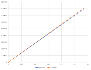
    Using VREF = 1.176, gain = 4, and VIN = 0.28358 V, I calculated your expected ADC code in decimal to be 8091297d. This means your expected value is higher than your measured value, resulting in a gain scaling coefficient >1. This is shown in the plot below

    Calculating "expected / measured" yields a gain scaling coefficient of 1.016374. Since the gain scaling registers use a 24-bit, unsigned value, you can multiply this coefficient by 2^23 to get the value in decimal (8525964d) and then convert to hex (82188Ch). This is the value you would write to the gain scaling register

    -Bryan

  • Hi Bryan,

    I really appreciate your support and your patient. I will go ahead test it and let you know the results.

  • Hi Amir Eshragi,

    You are welcome, let us know what you discover

    -Bryan

  • Hi Bryan,

    Hope you had a good holiday. I would like to thank you for all your help. Everything worked out as you mentioned.

    Thanks

    Amir

  • Hi Amir Eshragi,

    Glad we could help!

    -Bryan