This thread has been locked.

If you have a related question, please click the "Ask a related question" button in the top right corner. The newly created question will be automatically linked to this question.

ADC128S102EVM: Reading ADC channels troubleshooting

Part Number: ADC128S102EVM
Other Parts Discussed in Thread: ADC128S102

Hello,

I got a ADC128S102EVM board and I am trying to communicate with the ADC using a ProAsic3e from Microsemi. 

For this, I removed the resistor R42 to use an external VA/VREF (3.3V in my case) and I added a wire to supply VD with ProAsic3e 3.3V. The PHI board is not plugged, I am currently not using it to communicate with the ADC. The SPI communication comes from the ProAsic3e and is connected on J26.

My problem is that I receive on DOUT the values of the ADC channel 0 regardless of the address (between b'000' and b'111') I try to send on DIN. However, if I send logicals 1 on DIN while CS is low, I got the value of the ADC channel 7. But it not the case if I send only b'111'. 

It looks like a timing problem but I have checked the control signals with an oscilloscope and they are following the protocol described on the ADC128S102 datasheet.

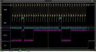
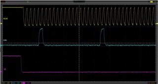
Here is what I send with the FPGA for reading the channel 1 of the ADC. (My probs are placed on J26)
I have checked that VA>=VD and it is the case.

I have first tested the ADC128S102EVM with the PHI board and the ADC128S102EVM GUI. In this case I can read every ADC channels without any problems. So the ADC128S102EVM is functioning correctly.

Any ideas of where there could be the problem?

  • Hi Doriane,

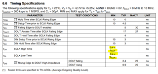
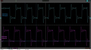
    Welcome to E2E! Thanks for your question and detailed post. I agree, it does sound like a timing issue. It seems the device is not able to distinguish the binary values of DIN and parses all the bits as all 0's or all 1's. Is your SCLK following the SCLK high and low minimum times listed in the datasheet section 6.6? In your scope shot, it looks like it might not be.

    Best,

    Samiha

  • Hi Samiha,

    Thanks for your reply. 

    Indeed, SCLK high time was too small. My SCLK frequency is 8MHz and my high time was under 50ns. I corrected it, now the minimum timings of SCLK are respected. I compared SCLK signals sent by the PHI board (using the ADC128S102EVM GUI) and by the ProAsic3e and I don't see any difference in timing.

    I think my SCLK signal is good now, but my problem is still here. I still cannot read any ADC channel other that 0.  

  • Hi Doriane,

    Thanks for your patience as we were out of the office for the holidays. It looks like your SCLK signal is correct now. Is DIN also identical to when using the PHI controller?

    Best,

    Samiha

  • Hi Samiha,

    Yes, DIN is identical to when using the PHI controller.

  • Hi Doriane,

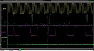
    Thanks for sharing. In that case, it may be something on the FPGA side. What SPI settings are you using (CPOL, CPHA)? What input are you applying? Could you please share an oscilloscope/logic analyzer measurement of DOUT data as well as SCLK, DIN, and CS?

    Best,

    Samiha

  • Hi Samiha,

    My SPI settings are CPOL=1 and CPHA=1

    In my current test I want to read channel 1 eight times in a row. I can see DOUT signal change only if I change voltage on AIN0. If I change voltage on AIN1 nothing happens on DOUT.

    My inputs voltages are: VA=3.3V, VD=3.3V and AIN0=3.29V (this voltages are measured, not only requered)

    Here is my measurements: 

  • By the way, I'm wondering if it is not an signal integrity problem? Could you confirm me that neither the eval board nor the PHI board have pull-up/pull-down resistor on CS, SCLK, DIN and DOUT. If yes, what are there values? 

    Best

  • Hi Doriane,

    Thanks for your response. There should be no signal integrity issues if the following high/low voltage limits are followed:

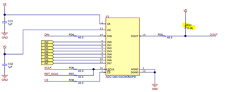
    However, I am just now noticing this pull-up in the EVM schematic on DOUT:

    However, I do not think this is the source of the issue as you are using the same EVM, which worked fine with the PHI. I do not see any additional pull-up/pull-down on the PHI board schematic.

    Let me look into the images you have shared and get back to you with more feedback.

    Best,

    Samiha

  • Hi Doriane,

    A few thoughts:

    1. Is your scope bandwidth limited, or are your digital signals really sawtooth shaped? I see your previous capture of SCLK. Just wanted to confirm that the actual signals are still keeping to timing specifications and are not being limited by your FPGA drive capability.
    2. You are sending multiple AIN1 reads in your scope-shot. Could you please try it with 2 AIN1 read commands in 1 frame (so raise CS high after the second DIN frame). This would help confirm that the DIN commands are being read correctly.

    Best,

    Samiha

  • Hi Samiha,

    Yes the sawtooth shaped is due to my scope. Here is the frame with 2 AIN1 read:

    I have checked CS voltage. For information CS high voltage is correctly at 3.3V and not at 2.4V as it seems to be on this capture. This wrong value is only due to my 4th prob that is not very precise.

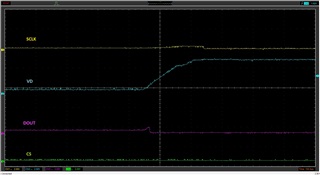
    Checking ADC power sequence I have noticed that DOUT follow VD when VD power up with the PHI board. But in my case DOUT start by following VD and then drop down.

    Then DOUT rise when SCLK and CS go to high value.

    Can that cause start up problem for the ADC?

  • Hi Doriane,

    Thanks for sharing the images. As this is an older part and the datasheet doesn't seem to mention much about the expected start-up behavior, I'm not sure. I would recommend trying to replicate the PHI controller behavior with DOUT if you are able. It is strange that it pulls low when there is a pull-up on DOUT. Looking at your screenshot again, I'm wondering if the clock is too noisy. I spoke to my team and I think we can narrow it down to your FPGA being unable to properly read DIN. I will try to recreate the scenario on my end early next week. It may be a phase issue with DIN not being properly aligned. Could you also share the same screenshot of all the signals when using the PHI board?

    Best,

    Samiha

  • Hi Samiha,

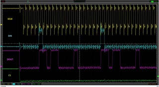
    Here is the screenshot of all signals when using the PHI board.

  • Hi Doriane,

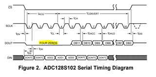
    Thanks for sharing this image. Interestingly, it looks like the PHI DOUT does have the expected first "four zeros" as shown in the datasheet timing diagram, attached below. Your ProAsic3e DOUT does not.

    This is signifying that your FPGA is likely not registering DIN at all. This may need debug on the ProAsic3e controller side. All your ADC input signals seem to be correct and following datasheet specifications.

    Best regards,

    Samiha

  • Hi Samiha, 

    Thanks for your help. I finally found a solution. I removed the resistors R34, R35, R36, and R37 and I connected directly my wires for SPI to the ADC. And I removed also the wires I was using for probing SPI signals. I think problem was caused by undriven wires.

    Best regards

  • Hi Doriane,

    Ah, I see, glad to hear it! Thanks for letting me know. I'll keep that in mind for future debugs.

    Best,

    Samiha