This thread has been locked.

If you have a related question, please click the "Ask a related question" button in the top right corner. The newly created question will be automatically linked to this question.

DAC8740H: Physical layer conformance testing ever pursued with this preliminary schematic?

Part Number: DAC8740H
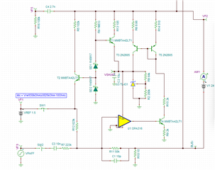
Other Parts Discussed in Thread: DAC8742HEVM

Has any FF physical layer conformance testing been performed on this preliminary circuit? 

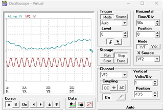
I have been simulating some conditions with the DAC8740H PAFF Discrete Loop Powered Transmitter Simplified TINA simulation as a starting point from another forum thread, but I am not obtaining the amplitudes or slew rates I would expect to pass these compliance tests. 

  • Hi Calvin, 

    Joe will be able to provide more information on what testing has been done when he returns from holiday break (likely next week). 

    Best,

    Katlynne Jones

  • Calvin,


    I'm still out of the office, and I'll be out most of this week as well. However, I did see your question come in and I thought I'd give a quick answer. I assume that you are referring to this e2e post on using the DAC8740H with PAFF:

    https://e2e.ti.com/support/data-converters-group/data-converters/f/data-converters-forum/663222/dac8740h-profibus-fieldbus-schematic-with-the-tm4c123/2436949

    To my understanding, we did start running tests with this schematic. We had contracted with a third party to run tests and I did find some log files for some PAFF tests. I'm not sure if they ran a set of physical layer tests, and I'm also not sure what was completed.


    Joseph Wu

  • Hello, yes that is the post I was referring to. After working further with the simulation, I did manage to get something that seems to follow what I am measuring on the output of the DAC8742HEVM kit which seems more promising. I am comparing these results to a test clause data sheet I found, and it seems the slew rates and amplitudes I am receiving in the current simulation could meet the criteria listed on the document I found. 

    I would like some more information, if it can be located, on what was pursued testing wise previously and if the circuit had many modifications to pass the conformance testing. Or, if there is no more information that can be located, then why was the testing not pursued further? Did the funding for the project get dropped? 

    I plan to do a layout with the simulated schematic to see how it performs on FF but would like to know if there are any major issues or concerns you would have before I pursue this.

  • Calvin,


    I'm was in today, but I'm out again tomorrow before coming back next week.

    The previous testing pre-dates me being in this particular group. The testing was spearheaded by a system engineer that left the group. It's likely that it was dropped when he left, and that so much time had passed since the original introduction of this device that it was just deemed not important enough to continue the PAFF registration.

    To be honest, I'm not as familiar with Foundation Fieldbus circuits and protocols as I am with HART, so I'm not sure I have much to add to these schematics. I'll root around through the material I have and see if there's any more that I can add to this thread that isn't proprietary to the company that started this development.


    Joseph Wu

  • Calvin,


    I did some digging into the PAFF circuit. I found an email from someone (no longer at TI) about the PAFF development and he said that their circuit passed all of the physical layer tests except one. He said that it had missed a "specified input impedance frequency response" test. He didn't remember enough details to know exactly what the issue was but he does remember that they had a few ideas in mind to fix it. However, he wasn't sure if the final version of the Altium project captured this adjustment or not.

    Again, I'm not familiar with PAFF and it's tests, but this description might be similar to the HART transmitter test for out-of-band interference. In those tests, different out-of-band frequency noise of different amplitudes is applied to the loop and the device should reject the noise. If it is similar, then this is a question of different resistors and capacitors at the MOD_OUT, MOD_IN, and MOD_INF pins of the device.

    Sorry I couldn't be of more help on this question. Let me know if you have any other questions about the device.


    Joseph Wu

  • Calvin,

    I did find one short app note on designing PAFF:

    https://www.ti.com/lit/pdf/sbaa367

    It's not a lot of information, but it does show they continued to look at the schematic.

    Joseph Wu

  • Thank you for looking into this!