Other Parts Discussed in Thread: LMK00301, LMK04832
hello:
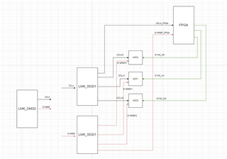
I am planning to synchronize multiple AFEs with JESD204B. Currently, I encountered some issues in PCB design as shown in the picture. I am using LMK04832 to output DEVICE CLK and SYSREF signals, and then fan them out to AFEs and FPGA through LMK00301. I known that each group of DEVICE CLK and SYSREF signals should be length match such as dclk0 and sysref0. Question is, should DCLK0, DCLK1, DCLK2 also be length match or unnecessary? And for the sync_n signals output from FPGA, such as sync_n0 and sync_n1, do they need to be length match?
thanks