This thread has been locked.

If you have a related question, please click the "Ask a related question" button in the top right corner. The newly created question will be automatically linked to this question.

ADS8166: ADS8166

Part Number: ADS8166

Hello,

I am implementing the ADSB166 in my system and we are having trouble reading data from the registers. So far we are checking that we correctly write to the registers and that we can read it afterwards but for some reason when we perform the read operation the MISO line returns illogical values (I assume they are measurements). 
The code performs the following:

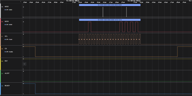
- First send a 24-bit frame for writing to the REG_ACCESS Register the REG_ACCESS_BITS = 1010 1010b.

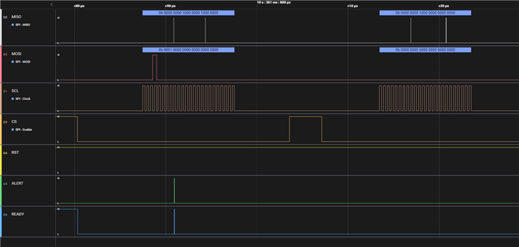
- Second we read from that same register with a 24-bit frame with the read command and it should return 1010 1010 0000 0000 0000 0000, but instead we recieve the values mentioned before.

Please find attached the signals received:

GLOBAL TRANSACTION:

WRITE COMMAND:
READ COMMAND:

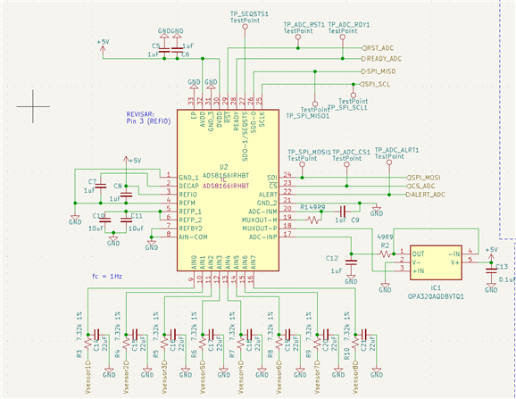
I am also adding the schematics in case there is something wrongly connected:
Thank you for your assistance 

  • Hello Victor,

    Thank you for your post.

    The REG_ACCESS_BITS in register 00h must be written by using the normal WR_REG command frame. This means you must write a data value of "1010 1010b" to address 00h using the register write command as follows:

    WR_REG 11-bit address  8-bit data

         0000 1  000 0000 0000 1010 1010 = 0x0800AA

    In the second frame, you must send the RD_REG command frame using:

    RD_REG 11-bit address  8-bit data

         0001 0  000 0000 0000 0000 0000 = 0x100000

    In the third frame, you can hold SDI low and send at least 8 SCLKs (i.e. NOP command). The requested register data will be output in the first 8 bits on SDO:

    Regards,

    Ryan

  • Hello Ryan, thank you very much for your reply,

    If I am not mistaken, the screen captures that I attached follow the behavior you describe yet in the third frame I am unable to see the requested register data in the first 8 bits, do you know what could we be doing wrong? or do you need more information on how we are doing it? 
    Thank you.

    regards,

    Víctor 

  • Hi Victor,

    My apologies, I couldn't load the images properly before my last reply. Your logic analyzer captures look correct for SDI. For SDO, there appears to be some glitches occurring much faster than one SCLK period.

    In your schematic, I noticed that REFBY2 is shorting to ground. By default, the internal REFBY2 buffer is powered on and you must write to the device to turn it off. I suggest removing this connection for now, if possible. This pin can remain floating.

    Regards,

    Ryan

  • Hello Ryan, 

    Thank you for your reply, we were able to modify timing according to SDO specifications and now the communication is correct.

    Regards,

    Víctor 

  • Hi Victor - glad to hear you resolved the issue! Let us know if you need further assistance.

    Regards,

    Ryan