This thread has been locked.

If you have a related question, please click the "Ask a related question" button in the top right corner. The newly created question will be automatically linked to this question.

ADS1248: Data converters forum

Part Number: ADS1248
Other Parts Discussed in Thread: STRIKE

Good day,

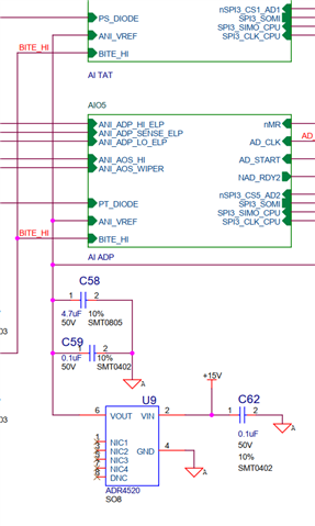
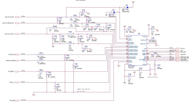
We use the ADS1248 in our design and the device is supplied with bipolar voltage of ±2.5V, IEXC1 excitation current is 1mA, and reference voltage 2.048V.

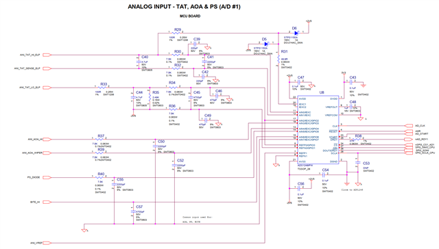
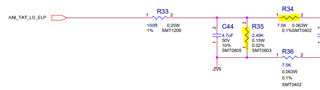
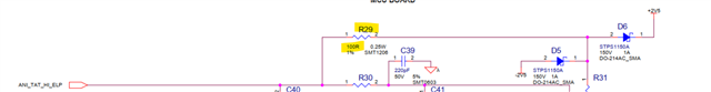
The max analog input protection on each channel are assured by either TVS5.0SMJ20CA, or VS-MBRS1100-M3/5BT, as shown in the schematic captures below:

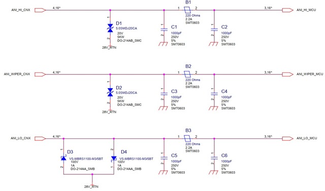
We're looking for advises from TI experts to see the correctness and adequacy of this implementation to protect the device from lightning transients Pin Injection Test Waveforms A, Level 4:

  1. Waveform 3, Level 4, VOC/ISC = 1500V/60A, DO-160G Figure 22-3, 1 MHz
  2. Waveform 4, Level 4, VOC/ISC = 750V/150A, DO-160G Figure 22-4

Thank you very much for helps.

Chuck.

  • Hi Chuck Wong,

    We do not have any expertise with these specific tests (lightning strikes for avionics) so I cannot give you any specific actions to take to pass them. However, typically we would add TVS diodes to eliminate transients and current-limiting resistors to limit the current into the ADC pins (as per absolute maximum ratings) in the case of a sustained overvoltage event. Your board appears to meet both of these requirements already, assuming you have selected component values to respond to the specific transient events you expect your board to see.

    I would just make sure you have these components on all of the ADC pins that are exposed to the inputs. For example, I am not sure where the "ANI_VREF" net goes, but if that went to a terminal block that is exposed to the outside world, you would want to ensure that this pin is also protected from transients and overvoltage events

    You can also review our Precision Labs content on electrical overstress: https://www.ti.com/video/series/precision-labs/ti-precision-labs-analog-to-digital-converters-adcs.html, which is highlighted in the image below

    -Bryan

  • Hello Bryan,

    Thank you for your reply.

    To answer your questions:

    • ANI_VREF is an internally generated reference voltage. It is not exposed to the outside.
    • All ANI are protected with TVS diodes and current limiting resistors.

    In the design of our UUT, there are two ADS1248 devices configured in the exact same manner as in the provided schematics. Our troubleshooting efforts of the failed UUT have confirmed that the ±2.5V supplies were no longer valid following pin injection testing. Additional investigation has revealed that:

    • The ±2.5V remain invalid if one of the two ADS1248 was removed from the board.
    • The ±2.5V become valid when both ADS1248 were removed from the board.
    • We think that both ADS1248 devices were fried as the result of the tests.

    As you may see in our schematics, we use the A/D internal excitation current (of 1mA) for the excitation of RTD circuit at pin IEXC1, and this line is unprotected by current limiting resistors up to the input ANI_TAT_HL_ELP (this latter was protected by TVS).

    1. Could this be the problem of overcurrent from the input ANI_TAT_HL_ELP, thus damaging the ADS1248?
    2. If we want to add current limiting resistors between pin IEXC1 and the RTD circuit, how do we control the excitation current value of 1mA?
    3. Is the current output at IEXC1 pin autoregulated, so external current limiting resistors won't affect the output?

    Thank you!

  • Hi Chuck Wong,

    Yes, it is possible that the ADC was damaged due to large currents on the IDAC pins, since those are not current limited in your system

    You can place a current-limiting resistor in series with each IDAC pin, but note that the IDAC has a "compliance voltage" specification in the datasheet that must be met to ensure constant current. This resistor will increase the total resistance between the IDAC output pin and ground (AVSS), so you might need to reduce the IDAC current in order to meet the compliance voltage.

    -Bryan

  • Hi Bryan,

    This is an old post of exchanges between you and Sabine, but she is no longer working here with us today: https://e2e.ti.com/support/data-converters-group/data-converters/f/data-converters-forum/992661/ads1248-rtd-3-wires-circuit/3666554#3666554

    With reference to the above and the previous version of the schematics below, I don't understand her reasoning for asking her question regarding the 100Ω, then your suggestion to remove the R29, 100Ω current limiting resistor. In the process, she had also removed the R31 in series to the IEXC1 pin.

    Those components were there for the lightning protection (LP).

    Any explanation on her motive, then your subsequent suggestion?

  • Hi Chuck Wong,

    In the case of Sabine's circuit, the highlighted resistors below act as the current limit for the REFP/REFN pins. The 100 ohm resistor (specifically R33) didn't do anything as far as I could tell, and was impacting the measurement

    I am not sure why the resistors on IEXC1 were removed, this was not my recommendation.

    -Bryan

  • I do believe that the question was on the R29 (100Ω, current limiting resistor), but not R33:

  • Hi David Wong,

    This was not my understanding at the time. Also, those resistors are not strictly necessary if the inputs are controlled and there is no expectation of overvoltages

    Now that you have explained the type of system you are designing, those resistors are likely necessary protection components. And they probably need to be greater than 100ohm, though I leave this to you to determine based on the amount of protection you require as well as the IDAC compliance voltage

    -Bryan

  • Hi Bryan,

    Getting back to the lightning protection for the ADS1248 device excitation current output IEXC1 line, by installing current limiting resistor, could you point me to where I can find the maximum voltage/current that the ADS1248 device is capable to support without damaging it?

    We're trying to determine the value of the resistor.

    Thank you!

  • Hi Chuck Wong,

    Please use the absolute maximum ratings from the ADS1248 datasheet (section 7.1). This provides the upper limit, but you should try as best as possible to keep the voltages / currents away from these ratings continuously. For example, I might target a current limit of 2-5mA, instead of the 10mA listed in the datasheet, to provide a lot of margin in your design

    -Bryan

  • Good day Bryan,

    Sorry I have to get back to this post, we still need your helps and hoping that we will find a solution to our problem. Thank you for your patience.

    Yeah so with reference to the first schematic in my first post above with the U8=ADS1248 installed, we have 2 such circuits implemented in the exact manner. The other ADS1248 is labeled as U1. Analog inputs to each A/D are independent signals (no link between them). 

    Those two "identical" circuits are completely separated in the design, the common points linking them are:

    • +2.5V (AVDD)
    • -2.5V (AVSS)
    • +3.3V (DVDD)
    • Analog reference ANI_VREF (2.048V) connecting to REFP1 pin

    For monitoring purposes, the above voltages are continuously been monitored by the MCU integrated A/D peripheral of the TMS570LS so we have a realtime view on them all the time.

    While our previous discussions are on the protection against pin injection on the U8 IEXC1 pin. Now I have this question that is scratching big time, not related in solving the protection issues, but more on the functioning of the ADS1248. Please let me explain.

    We performed pin injection testing on U8 pin IEXC1 (ANI_TAT_HI_ELP) and pin ANI1 (ANI_TAT_SENSE_ELP), separately of course. Every time when the test failed on the U8, it looks like U1 was affected too. Below are our observations.

    Immediately after failed pin-injection on U8 input:

    • +2V5: 0.7661 instead of 2.5 V
    • -2V5:-1.6614 instead of -2.5 V
    • REFP1: 1.6384 instead of 2.048 V
    • SPI working fine: U1 and U8 configuration registers accessible and hold correct values (SYS0, OFCx, FSCx, IDACx etc.)

    Replacing U8, REFP1 recovers to good level, but:

    • +2V5: 1.2463 instead of 2.5 V (changed)
    • -2V5:-1.6614 instead of -2.5 V (unchanged)
    • SPI working fine: U1 and U8 configuration registers accessible and hold correct values (SYS0, OFCx, FSCx, IDACx etc.)

    Removing U1 (not subject of the pin injection test): 

    • All supplies return to normal levels
    • U8 is operating normally without U1 installed
    • SPI working fine: U8 configuration registers accessible and hold correct values (SYS0, OFCx, FSCx, IDACx etc.). U1 registers are all 0xFF (device absent).

    Replacing U1, all operating correctly.

    What puzzles us are:

    1. How could failed pin-injection tests on U8 affect U1?
    2. How U1 and U8 affect the supply voltages when failed (+3.3V remains at good level all the time)?

    Thank you Bryan!

  • Hi Chuck Wong,

    What generates the REFP1 (2.048V) voltage? Is that a discrete reference? If so, can you send the schematic?

    ANI_TAT_HI_ELP is connected directly to the supply voltage as well as IEXC1. Is it possible the test current is getting into the supply? That would seem like a reasonable explanation as to why the pulse is affecting both devices. Can you share the power supply schematic as well?

    Is there still no protection on IEXC1? The schematic I have does not show any, but perhaps you have made updates since then

    -Bryan

  • Hi Bryan,

    Thank you for the prompt reply.

    1) Schematic for the REFP1 2.048V below:

    2) Yes that was in my mind, but on our latest test, ANI_TAT_HI_ELP hasn't been exercised by strike, so wondering where could be the path.

    3) Not yet implemented on the IEXC1. We want to see other analog input pins before changing the board hardware and found this problem (both ADS1248 always grilled together).

    Please remember that once the both ADS are replaced, no more 2.5V problems, so wondering also what is the state of the ADS when it failed, holding the ±2.5V hostages.

  • Hi Chuck Wong,

    In your previous post you said:

    We performed pin injection testing on U8 pin IEXC1 (ANI_TAT_HI_ELP) and pin ANI1 (ANI_TAT_SENSE_ELP), separately of course.

    Are you saying you retested the boards (after replacing U8 and U1 I assume) and then did not perform the injection test on ANI_TAT_HI_ELP?

    The first scenario you described makes sense: you hit an unprotected pin with some large transient voltage. This caused the ESD diodes on that pin to turn on, and probably sink too much current causing them to short out (and permanently damage the ADC). Therefore, you needed to replace both ADCs in order for the system to return to full functionality because in both cases you (likely) had shorts inside the ADC that were also shorting out your supplies.

    If you performed a different set of tests on different pins, it would be helpful to know what you changed and what the result was.

    -Bryan

  • Are you saying you retested the boards (after replacing U8 and U1 I assume) and then did not perform the injection test on ANI_TAT_HI_ELP?

    Exactly right. The ANI_TAT_HI_ELP pin was not retested after replacing U8 and U1. We continue to test the SENSE pin. What I want to highlight here is "pin injection to any of the two separate analog input pins on U8 was having the same consequence: U1 not working". 

    While I understand your explanation on the ANI_TAT_HI pin (protected only using TVS in the ELP board), U8 damaged by high transient current because of internal ADS EDS protection diodes to break down. How could this current also damage the internal EDS protection diodes inside the U1 IEXC1 pin?

    Similarly, I cannot find a reason on high current on the U8 ANI_TAT_SENSE pin to damage somewhere on the U1.

    The ±2.5V generation was not affected by the strike, and resumes working fine following U1 and U8 replacement.

  • Hi Chuck Wong,

    It is possible the strike got into the supply or grounding that is shared by the ADCs and caused an issue that way. I'll be honest, it will be very difficult to identify a root cause remotely. Even if I had your board in hand as well as the board files, this would be a challenging task (as you are clearly aware)

    Are you able to lift some of the ADC pins and perform the tests again? For example, if you are injecting at U8 ANI_TAT_SENSE, try removing R32 and seeing what happens. My guess would be that you don't see an issue, but if you do then you know you have a leakage path somewhere. Or try injecting at U8 ANI_TAT_HI_ELP, removing R30, and lifting pin 20 on the ADC. This injects the transient into your supply through D6. Does this cause an issue with U8? What about U1?

    If you don't have U8 populated but strike the same locations near U8, do you see a failure at U1? If you strike the same locations but this time at U1, does this cause U8 to fail?

    Ultimately, you need to try combinations of configurations to determine how the fault current is getting into the ADC. Maybe it's not what seems obvious.

    -Bryan

  • Hi Bryan,

    Yeah I see that would be months of works ahead if we want to pinpoint the issues, and that won't contribute to resolve the ultimate problem here. At the end of the day the main task remains protecting the circuit by preventing the strike energy to travel all the way to the A/D locations, therefore we're going to concentrate our efforts on it.

    As we both can see, both ±2.5V voltages were impacted when the U1 and U8 goes bad. Do you have any insights as on why the ADS1248 is holding down their supplies to a bad level?

    Also, if we want to simulate an input to the ADS1248 with a circuit breadboard to measure the traveling current, what is the typical impedance of an input to the A/D that we should use?

    Thanks again!

  • Hi Chuck Wong,

    As we both can see, both ±2.5V voltages were impacted when the U1 and U8 goes bad. Do you have any insights as on why the ADS1248 is holding down their supplies to a bad level?

    If the ADCs are holding down the supplies, and a power cycle does not eliminate the issue (and only replacing the ADCs does), then the ADCs were damaged in such a way that likely caused a short internal to the device. That short is likely to AVSS, AVDD, or both, which caused your supply voltage to sag. I wonder if you would see different behavior if you were using unipolar +5V supplies instead of bipolar.

    Also, if we want to simulate an input to the ADS1248 with a circuit breadboard to measure the traveling current, what is the typical impedance of an input to the A/D that we should use?

    See section 9.3.2.3 in the datasheet (Analog Input Impedance). Note that this is for the analog inputs that are fed into the PGA. The VREF input currents are specified in the Electrical Characteristics Table, and can considered as correlating to the input impedance e.g. 1uA @ 1V = 1Mohm input impedance.

    I don't have a model (or heuristic) to share with respect to the IDAC input however

    -Bryan

  • Thank you so much for your prompt helps Bryan!

    You've so far demonstrated great knowledge, along with willingness to help ... which are truly appreciated here Slight smile

  • Hi Chuck Wong,

    I am glad we could help you

    -Bryan