This thread has been locked.

If you have a related question, please click the "Ask a related question" button in the top right corner. The newly created question will be automatically linked to this question.

ADS1274: Spi configuration

Part Number: ADS1274
Other Parts Discussed in Thread: ADS1278EVM-PDK

Hi team, 

        Power up ADS1274  DVDD->IOVDD->AVDD->VREF->FCLK in this order.

After the power up in spi protocol data DRDY pin is which state high or low ?

while doing  this project the DRDY is no resposne (inital conditiuon low ,after start the conversion there is no response)...

please clarify the questions.....!

Thanks and Regards,

Aravind.SR


  • Hello Aravind,

    After power-up, CLK input active, at least one of the ADC channels in power-up, and the /SYNC pin pulled high, the /DRDY pin will toggle at the output data rate, which depends on the configuration of the CLKDIV and MODE pins.

    Please send a picture of your schematic showing all connections to the ADS1274 and I will review.

    Regards,
    Keith Nicholas
    Precision ADC Applications

  • Hi Keith Nicholas,

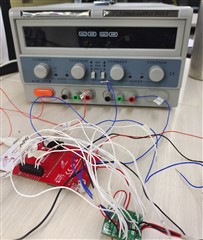
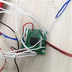
    In this adc1274 is implementing in breakout board.

    After the power up,clk input active,i enable the PWDN1 for channel 1 output,and the SYNC pin pulled high after that DRDY pin is no response. 

    Regards,

    Aravind

  • Hello Aravind,

    This breakout board is not going to work.  You need to design a custom board that includes all bypass capacitors, reference, and input amplifier on a single board with a solid inner ground plane for proper operation.

    Please refer to the ADS1278EVM-PDK user's guide for an example layout.

    https://www.ti.com/lit/pdf/sbau197

    Regards,
    Keith