This thread has been locked.

If you have a related question, please click the "Ask a related question" button in the top right corner. The newly created question will be automatically linked to this question.

ADC09QJ1300EVM: ADC09QJ1300EVM related issues

Part Number: ADC09QJ1300EVM
Other Parts Discussed in Thread: TSW14J57EVM, , LMK04828, LMK00304

hi,

The customer used ADC09QJ1300EVM and TSW14J57EVM for testing and verification, and encountered some problems. Please help solve them. The problem description is attached.

ADC09QJ1300EVM related issues.docx

Thanks!

  • Hi Jeno,

    I am checking on this and will get back to you soon.

    Thanks, Amy

  • Hi Jeno,

    We are still looking into this. I think you answered your first question and regarding the last question, "Waiting for user input" in HSDCPro is just what shows up when it is idle and the software is waiting for command, such as clicking "Capture". 

    This error though may have to do with SYSREF coming from the FPGA. We will continue to debug this and provide an update by Tuesday next week.

    Best regards,

    Drew

  • Hello,

    Is FPGA debugging completed? Are there any firmware updates?

  • Hello Jeno,

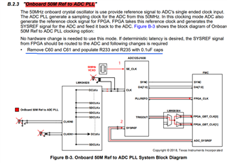
    From the document you shared it looks like you are using the on board 50 MHz reference. This particular mode of operation has some tricky features.

    From the screenshot you shared we can see that the FPGA_GBT clocks come from the ADC TRIGOUT pins. The way this mode works is internal to the ADC the the cpll will generate the converter clock, the s pll will generate the serdes clock and the trigout will take the serdes clock and divide it down to output the fpga clocks. However, there are only 3 options for divisors for the trigout, 16, 32, 64 and none of these dividers are valid default divisors for standard fw that works with HSDC Pro. This is why you are seeing this error. 

    There are two ways to solve this problem...

    Option A)

    Continue to use the onboard 50 MHz reference to generate the adc clock but use the LMK to generate the reference clock. If you choose this you will have to provide a clock input to the LMK04828 pins on sma pin J31, additionaly you will have to program the LMK04828 and LMK00304 to correctly generate the FPGA reference signals and route them to the FMC connector. This will be similar to external clocking mode of the adc.

    Option B)

    There is firmware to support this mode on the TSW14J58 capture card with HSDC pro link to get https://www.ti.com/tool/TSW14J58EVM

    If this option is of interest I can share more detailed setup descriptions and an ini file for configuring the part.

    Best,

    Eric