This thread has been locked.

If you have a related question, please click the "Ask a related question" button in the top right corner. The newly created question will be automatically linked to this question.

DAC39RF10EVM: J12 Jumper Alternative

Part Number: DAC39RF10EVM
Other Parts Discussed in Thread: SN74AUP1G125, , LMX1204, LMK04828

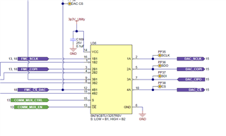
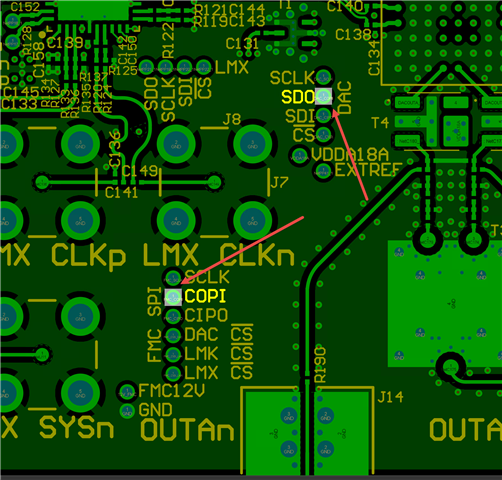
I noticed in the user manual that the ability to use SPI signals from the FMC+ connector will be supported on the next rev of the board. Is there a workaround for the current rev of the board to use the SPI signals from the FMC+ connector?


  • Hey Joshua, 

    We do not have firmware to support SPI control via the FMC as of now; however you can route the SPI signals from the FMC to the DAC/LMK and LMX on the current board. All you need to do is populate jumper J12.I am not sure why it mentions this being supported on the next revision of the board. 

    Thanks and Regards, 

    Matt

  • Hi Matthew,

    To follow up on this, I tried to program the EVM via SPI over FMC+ after populating jumper J12 but was unable to do so. While following the DAC's user guide, I tried to read the FUSE_DONE register and received 0xFF instead of 0x1. My testing so far seems to indicate that the SPI signals are not being received by the EVM properly. I'll perform some more testing but I have a couple of questions:

    • Can you confirm that the pinout of the SPI signals to the FMC+ connector are correct in the Rev A. schematic?
    • Are there any other steps required to switch to SPI over FMC+ other than populating J12?
  • Hi Evan,

    I have attached the schematics for the board so you can confirm the pinout. Shorting J12 headers is all that is needed to mux over the LMX, LMK, and DAC's SPI signals from the FTDI to the FMC+ connector. 


    DAC39RF10 EVM_RevA2(001)_Sch_2023-02-21.pdf

    Thanks, Chase

  • Hi Chase,

    I was able to verify the pinout to the FMC+ connector and was able to pass signals through to the EVM. I have noticed that when I try to drive FMC_CS_DAC low from the FPGA, the probe point reads ~0.025 V instead of 0V. Based off the datasheet for the SN74AUP1G125, this voltage should be low enough to register as a low-level input to pass the logic through from the DAC_CIPO to the FMC_CIPO but probing the FMC_CIPO reads 1.8V while the DAC_CIPO reads ~0.057 V. Note: The probe points for DAC SDO and SDI look to be swapped in the schematic.

    It seems like the pull up resistor to 3.3V connected to the 1.8V signal is preventing the FMC DAC chip select from functioning properly. Do you know if the chip enable has to be connected to ground (0V) to enable that data path?

  • Hey Evan, 

    That pull up should be going to 1.8V. If you wouldn't mind try removing that pull up, it should still work fine if the FPGA's output is a push pull CMOS output. I'll make sure to take note of this to correct our EVM's going forward. 

    CSb is usually high when the device is not being written to, which is probably why it was put there. Some devices do not tri-state when they are not being read from, hence the addition of the tri-state buffer. Regardless as long as the CS coming form the FPGA is push pull its not needed. 

    Regards, 

    Matt

  • Hi Matthew,

    Thanks for the quick reply. I'll add that to the list of things to try. While talking with a peer, they also pointed out that it looks like there will be contention between the U30 level shift A3 output and the U34 buffer output when trying to communicate with the DAC. The outputs of the U29 and U32 tri-state buffers should be set to high impedance since the LMX_CS and LMK_CS would be asserted high. The pull up resistor R150 would then the B3 pin of U30 to 3.3 V so the A3 output of the level shift would always be 1.8V when neither the LMX nor LMK are selected right?

  • Hi Matt,

    To follow up on my last reply, we removed that pull up resistor and are still unable to read from the DAC over SPI. 

    Another observation we made is that neither PP36 nor PP37 for DAC_COPI and DAC_CIPO seems to react to the FMC_COPI signal.

    When FMC_COPI is driven high by the FPGA, the FMC_COPI (PP28) probe point reads 1.8 V, the LMK_SDI probe point (PP27) reads 3.3 V and the LMX_SDI probe point (PP20) reads 3.3V, mostly as expected. According to the schematic, PP20 for LMX_SDI is after a 3.3V to 2.5V level shift so that seems like it should read 2.5V, but all of the probe points indicate a high logic value. When FMC_COPI is driven low, FMC_COPI, LMK_SDI, and LMX_SDI probe points read 0V.

    No matter what FMC_COPI is driven to, DAC_COPI and DAC_CIPO probe points read 0.057 V. Do you have any information on why these probe points don't seem to be reacting as expected or the possible double driver of the FMC_CIPO signal that I brought up on Thursday?

    Thanks,

    Evan

  • Another follow up,

    After looking through the gerber files, it looks like FMC_COPI signal is not connected to pin 3 of U36 (pin name 2B1).

    In the gerber layers, that pin is not connected to anything.

    Thanks,

    Evan

  • Evan,

    The issue, as you have seen, is that the COPI pin is not routed on the mux.  I was looking at the schematic and layout and have something for you to try.  There are probe points on the FMC COPI and the DAC SDO pins.  Soldering a jumper wire between these two points should allow SPI transactions if the FPGA edges don't have too many reflections on them.  

    Below is a pic of the two probe points on the EVM.  Let us know if this fixes your issue.

    Regards,

    Geoff

  • Hi Geoff,

    We tried out soldering the DAC_SDO and FMC_SPI_COPI testpoints and still could not read data back from the DAC, likely due to the possible double driver case of the FMC_SPI_CIPO that I mentioned previously. We then soldered a jumper wire between the DAC_SDI testpoint and one of the FPGA GPIO points located at the bottom right of the EVM board. With both of these jumper wires, and R163 removed as previously suggested, we are able to confirm writes and reads to the DAC.

    Thanks,
    Evan

  • Hi Geoff,

    We are able to communicate to all three devices via FMC SPI using the modifications outlined in my last reply. However, we've noticed that the clock does not seem to be programmed properly on every try. Let me know if this should be moved to a separate discussion topic.

    We have the clock connected to a debug LED on our FPGA that is meant to toggle once per second and in some programming attempts, the clock is running slightly faster than expected. This results in errors of our other logic that uses the clock received from the DAC EVM board. I have a script that reads out all of the SPI registers of the DAC, LMK, and LMX devices and there are no differences in the register values between a "successful" EVM configuration and "unsuccessful" EVM configuration.

    To further debug this, I switched back to the DAC39RF10EVM GUI v2.0.37 programming method and was able to replicate the issue there. I programmed the DAC EVM using the same settings each time and sometimes the clock received by the FPGA was what we expected, but other times it was not. In order to rule out the board modifications causing problems, I switched to a different board and observed the same behavior.

    Note, the path of the clock in our FPGA is as follows:

    DAC_FMC connector -> transceiver input buffer -> general clock buffer -> register

  • Hey Evan, 

    I think I know what the problem is..

    The LMX1204 has a really strange quirk in that it reads back 2 less than what is programmed in the SYSREF_DIV and LOGICLK_DIV registers. If you did a register dump from the LMX1204 in a working state than the register map file you got likely has wrong values for these fields. SYSREF_DIV is in register 0x10 and LOGICLK_DIV is in register 0x09. 


    One easy way to see if this is the issue is just to add 2 to both register 0x09 and register 0x10 in your working dump and see if that fixes your issue. 

    Regards, 

    Matt

  • Just wanted to add,

    Just saw you had mentioned the clock is running slightly faster. That is likely exact the issue you are seeing as the divider is essentially being read back slightly less yielding a faster clock when you program that read back value the next time you use the device. 

    Matt

  • Hi Matt,

    The register values being written are based on the console output when programming the EVM via the GUI. Based on the console, these values come from a LMX1204.cfg and LMK04828 64b66b.cfg. The "expected" values that I compare against do come from reading back the registers via the TI GUI and as a result, these look to already account for the SYSREF_DIB and LOGICLK_DIV registers reading back 2 less than what is already programmed.

    Like I mentioned, this intermittent issue occurs both when configuring the EVM using the FPGA over FMC+ and when using the TI DAC EVM GUI. The register values for SYSREF_DIV and LOGICLK_DIV return the same values no matter what configuration and readback method, and if the clock is correct or running fast.

    Thanks,

    Evan

  • Evan, 

    Is there a way to measure the clock going to the FPGA? Could you give me some information on your setup so I can try to duplicate it using our in house firmware?

    Thanks!

    Matt

  • Hi Matt,

    Sorry for the delayed reply. There is not a simple/direct way to measure the clock going to the FPGA so instead we have the clock connected to a counter in our FPGA firmware. The counter has a max value based on the expected frequency of the clock and is connected to an LED that we have on the FPGA board so that the light should toggle once a second (one second on, one second off).

    We have a total of 8 LEDs and the others are connected to other clocks in our system in the same way. While trying to debug this issue, I noticed that the LED would toggle at different rates throughout the programming process of the LMK and LMX as the multiplier changed so I would program the EVM and then try to bring up the JESD link. I would then note if the JESD link was brough up successfully and then re-sync/reset all of the LEDs. In cases that the EVM programming and JESD link were brought up successfully, the LED corresponding to the clock received by the FPGA from the DAC EVM would toggle in sync with the rest of the LEDS. When the EVM was programmed and then the JESD link FAILED to connect, the LED for the clock from the DAC EVM would toggle slightly faster than the rest after the LEDs were reset/synchronized. After noticing this, I uninstalled jumper J12, and followed the same testing procedure of programming the EVM board, bringing up the JESD link, noting the status, and then resynchronizing the LEDS, but programmed with DAC EVM using the TI GUI instead of our FPGA firmware and was able to replicate the same behavior has mentioned before.

    Thanks,

    Evan

  • Hey Evan, 

    Just so I understand, You're saying the clocking going to the FPGA from the DAC EVM is sometimes slightly faster than it should be (LED in your setup is flashing slightly faster than once per second) and the link is not coming up? Could you send me a map of the registers you're programming to the LMX1204 as well as the DAC's sample clock and expected logic clk frequency? I can easily measure the logic clock/SYSREF of the LMX1204 in my lab. 

    Regards, 

    Matt

  • Hi Matthew,

    Attached is the set of registers being programmed to the LMX 1204. The DAC sample clock is 9 GHz and the expected logic clock is 70.3125 MHz.

    LMX1204
    0x00 0x0001
    0x5A 0x0000
    0x56 0x0004
    0x4F 0x0005
    0x4B 0x0003
    0x48 0x0004
    0x43 0x51CB
    0x41 0x65F0
    0x22 0x04C0
    0x21 0x0000
    0x1D 0x05FF
    0x1C 0x0A08
    0x19 0x0119
    0x18 0x0001
    0x17 0x6040
    0x16 0x0478
    0x15 0x0EF8
    0x14 0x0EF8
    0x13 0x0EF8
    0x12 0x0EF8
    0x11 0x0074
    0x10 0x1400
    0x0F 0x0B80
    0x0E 0x0002
    0x0D 0x0003
    0x0C 0x0000
    0x0B 0x0000
    0x09 0x0020
    0x08 0x0130
    0x07 0x0001
    0x06 0xC924
    0x05 0x493F
    0x04 0x3F11
    0x03 0x1F87
    0x02 0x0083
    0x00 0x0000

  • Hey Evan, 

    This configuration should generate a logic clock frequency of 70.3125MHz. From what you were saying, your FPGA is showing that this is not the case? 

  • Hey Matthew,

    Correct, it is not consistently generating a logic clock frequency of 70.3125 MHz. No matter what, the registers we read back from the LMX are the same, but the FPGA is not showing the same clock every time.