This thread has been locked.

If you have a related question, please click the "Ask a related question" button in the top right corner. The newly created question will be automatically linked to this question.

ADS124S08: ADS124S08

Part Number: ADS124S08

We are using TI ADC Module ADS124S08 which is a 24-bit module with 12 channels. We are facing some unexpected issues while writing its firmware. Following are the issues:

  1. The maximum ADC count we are getting is nearly 8388608 which is actually 23 bit maximum value. If it is a 24-bit ADC, its maximum value should be near to 16777216. I have checked the Register settings to configure ADC but I didn’t find any resolution based register. So how can we get 24-bit ADC counts for different voltages?
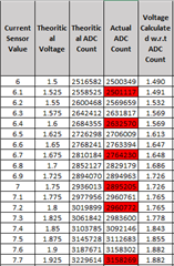
  2. Second issue we are facing is the ADC counts are more precise when we are giving 1.47 gain to ADC Channel (PFA-1) but when it is unity gain (PFA-4), the ADC counts are not that precise. In firmware, we are setting 2 registers – 0x04 with value 0x17 (for 100 SPS) and 0x02 with ADC channel. Attaching the analysis snap shot f.y.r (PFA-2&3).


Please get us the resolution of these issues and please let us know the changes required in our system.

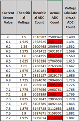
  •      ADC Counts Analysis 

  • Hi Nimish Palod,

    The maximum ADC count we are getting is nearly 8388608 which is actually 23 bit maximum value. If it is a 24-bit ADC, its maximum value should be near to 16777216. I have checked the Register settings to configure ADC but I didn’t find any resolution based register. So how can we get 24-bit ADC counts for different voltages?

    The ADS124S08 always measures differentially even when connected as single-ended.  This means that the output is always AINP relative to AINN.  The conversion result will be in binary 2's complement form.  Positive value codes will be from 0 to 0x7FFFFF (0 to 8388607).  Negative codes are 0xFFFFFF to 0x800000 (-1 to -8388608) when the input voltage at AINP is less than AINN.

    Second issue we are facing is the ADC counts are more precise when we are giving 1.47 gain to ADC Channel (PFA-1) but when it is unity gain (PFA-4), the ADC counts are not that precise. In firmware, we are setting 2 registers – 0x04 with value 0x17 (for 100 SPS) and 0x02 with ADC channel. Attaching the analysis snap shot f.y.r (PFA-2&3).

    I'm not sure what you mean by PFA.  Can you explain what you mean here?  The ADC PGA uses binary steps for the gain (1,2,4,up to 128).  There is no 1.47 gain.  Is this an external amplifier?  The full-scale range of the ADC is determined by the reference voltage used and the PGA gain ( 1 count = +/-VREF/PGA GAIN/(2^24 - 1).  If your measurement is single-ended (where AINN is connected to AVSS (AGND for unipolar supplies) then you are limited to a PGA gain setting of 1 and the PGA must be bypassed otherwise you will get a non-linear measurement.

    You need to make sure that the voltage input to the ADC is within the measurement range with respect to the PGA settings. To be of more help I would need to see the schematic and know all of the register settings that you are using.

    Best regards,

    Bob B

  • Hi Bob,

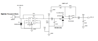
    Thanks for your reply. Please ignore the term PFA, it was added by mistake. The 1.47 gain was added externally (attaching the snap shot of circuit). The PGA is bypassed and we are working on replacing 1.47 gain to unity (attaching the snap shot of Unity gain circuit). 
    The system is working properly with 1.47 gain i.e. We are getting proper ADC counts w.r.t. Voltage input. But when we are shifting it to unity gain, the ADC counts for few voltages are not proper (attaching the snap shot of both the readings captured for 1.47 gain and unity gain). We are setting register 0x04 for 100SPS (register configuration - 0x17). We have tried reducing the Data Rate to 60,50 and 20 SPS, but the issue was still the same. Is there any other register required to be configured through firmware, since I tried with different register settings too but couldn't find the resolution. 

    Please find the attachments.

    Thanks and Regards,

    Nimish

  • Hi Nimish,

    This looks like it could be analog settling error.  You have your filter cutoff at 22Hz, but you are sampling in most cases much faster.  Even at 20sps output data rate you will basically see averaging over the 50ms period as the modulator sampling is at 256kHz.  Also, the same filter is on the input as it is on the output filter.  This will delay the settling even more.  The RC time constant is about 7ms, and for the 1/2 LSB settling you need about 17 time constants to fully settle for a 24-bit conversion.  This results in 120ms for full analog settling.  As you have two filters you elongate this time even further.

    In the end there is no advantage to collecting data faster than the filter response.  I can't explain the differences in the two circuits.  I would suggest verifying the settling behavior with an oscilloscope.  You may also want to verify the components used on the gain of 1 op amp to make sure that the values are the same as the 1.47 gain.  You could also try adding some delay or waiting an additional length of time before capturing the conversion result.  Sometimes collecting more than one result will also benefit by showing any settling issues.

    Best regards,

    Bob B

  • Hi Bob,

    As we have 15K series resistor and 47nF Capacitor mounted as low pass filter on both input and output side of OPAMP, making a cuffoff freq of 225Hz.

    Both the design for Gain=1 and Gain=1.47 is having same value parts.

    If it is an error due to settling period, then we would have observed similar results for 1.47 Gain channel.

    As a part of experiment, we removed the filter from both input and output of opamp but still no improvement observed.

    Let us know if you need any other specific information for this Issue.

    Thanks and Regards,

    Nimish

  • Hi Nimish,

    As you stated there really should be no difference between the two input configurations with respect to filter timing.  However there must be something different either with board layout, device configuration or communication. 

    • Please send me the register configuration being used in both the 1.47 gain case and the gain of 1 case. 
    • Also explain to me process of how you are measuring the input channel.  What I mean here is are you collecting only a single point of conversion of data, averaging several samples, etc.. 
    • Also tell me if you are cycling through the mux channels. 
    • Please also tell me how you are determining when to read the conversion data from the ADC.  Are you triggering an interrupt from DRDY, using a timer, etc.?
    • And do you read data direct or are you using the RDATA command to retrieve the conversion data?

    Best regards,

    Bob B

  • Hi Bob,

    To your queries:

    1. We are using same opamp for both 1.47 and unity gain. We are just replacing 2 registers for making it unity gain from 1.47 gain. So there shouldn't be any board layouting issue.
    2. We are configuring register 0x04 setting its value to 0x17 for 100SPS with Low Latency filter in both the cases (1.47 gain and unity gain). We tried configuring some more registers but there was no difference found. Also we tried lowering the data rate to 60SPS, 50SPS and 20SPS but the same issue was seen in all. Please let me know if we are missing any register to configure w.r.t gain settings.
    3. We are reading data directly using start and stop command and in between reading data register. Before that we are using wake up command to move on from stand by mode.
    4. We are taking average of 50 ADC counts. The attachment added above are showing ADC value of 50 readings average.
    5. We are reading 9 channels inputs on ADC. We are muxing channels configuring register 0x02 with channel numbers (from 0x0C to 0x9C).

    Hope you will understand our process of conversion from the following details.

    Regards,
    Nimish  

  • Hi Nimish,

    We are configuring register 0x04 setting its value to 0x17 for 100SPS with Low Latency filter in both the cases (1.47 gain and unity gain). We tried configuring some more registers but there was no difference found. Also we tried lowering the data rate to 60SPS, 50SPS and 20SPS but the same issue was seen in all. Please let me know if we are missing any register to configure w.r.t gain settings.

    Can you please send me the complete register map values you are using for each use case?  I would like to see more than just one register so that I can know what to expect from the ADC.

    We are reading data directly using start and stop command and in between reading data register. Before that we are using wake up command to move on from stand by mode.

    If you are using the START/STOP commands is the START pin set low from the micro GPIO?  And you still didn't answer my question regarding how you know when the conversion is complete and the data are ready to be read out of the ADC.

    We are taking average of 50 ADC counts. The attachment added above are showing ADC value of 50 readings average.

    Instead of sending me the average data, can you collect the data in such a way for me to see all of the conversion data?  Do you have a logic analyzer for me to inspect the communication flow and the data as it is being read from the ADC?

    We are reading 9 channels inputs on ADC. We are muxing channels configuring register 0x02 with channel numbers (from 0x0C to 0x9C).

    Can you verify for me what channels are gain of 1 and what channels are gain of 1.47?  Looking at your data again, I would expect the result to be much closer to the theoretical in both the 1.47 and 1 cases. What are you using as a source?  And how does that source differ between the two sets of data presented?  For the gain of 1 case there appears to be an unusual step error about every 3 readings and a significant non-linearity around 7.1 to 7.3mA.  In the gain of 1.47 data, you do not show this much granularity within the same data range so it is quite possible that the data would appear similarly if the same data points are used in each case.

    Best regards,

    Bob B

  • Hi Bob,

    According to the requirement, the program was developed for 1.47 gain and this is used from last few years which is working properly. In this firstly we set the Data Rate Register (0x04) Enbling low latency filter and 100SPS Data Rate (0x17 - configuration value). Then we set Input Multiplexer Register (0x02) with ADC input channel number (from 0x0C to 0x9C configuration value). Then we send Wake up command to ADC (0x02 - given on page65 of datasheet). We receive a GPIO interrupt when the data is ready or conversion is happened after which we read the Data output from ADC. At last when all the 3 byte data is received, we send Stop command to ADC (0x0A - given on page65 of datasheet). Rest all the registers must be set to default since they are not used.

    For unity gain, we tried configuring offset calibration register (0x0A to 0x0E) with value 0x00 and 0x0F to value 0x40 but no difference was observed. We tried using internal reference (Reference Control Register 0x05) and there we were getting proper values for unity gain but it was just till 2.5V. To cover full scale range still we couldn't find any solution.

    To your queries:

    1. START/SYNC Pin is set low from microcontroller GPIO. We receive the data ready information through GPIO interrupt whenever the conversion is completed. 
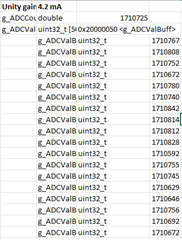
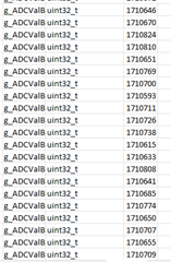
    2. I have captured the values used for averaging in a buffer for 4.2mA reading. Attaching the snapshot of the same f.y.r.

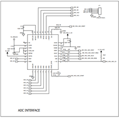
    3. AIN0 and AIN1 are set to 1.47 gain, rest all channels are set to unity.
    4. The source we are using is 0-20mA current simulator. The snap shot that I attached earlier is for nearby voltage readings for both the cases. 

    Please let me know if any more information required.

    Thanks and Regards,

    Nimish

  • Hi Nimish,

    Thank you for the information on the process you are using.  The process looks to be ok to me.  Let's back up a few steps.  First of all you are measuring the current based on the voltage response.  You are taking measurements based on the expected voltage outcome as opposed to the measured current.  The problem with this method is the currents that are used as inputs do not reflect the same overall response for both configurations.  The reason being is that in one case you are inputting a completely different set of currents where we don't know how linear your current simulator is across all steps.

    If you want to continue with the same approach , then you need to measure the actual input voltage (and you should probably do this anyway) and compare to the conversion result.  To accurately check the linearity you should also measure the reference voltage.

    If you plot your results as a linearity plot you can determine how close you are to the result with respect to the measured input value.  What we don't know is how linear your simulator is across all currents.  Some of the intermediate values you are using may show some error not due to the ADC but due to the simulator.  That is why both 1.47 gain and gain of 1 should use the same current as input as opposed to theoretical voltage as you have not actually measured the voltage.

    Best regards,

    Bob B