Other Parts Discussed in Thread: ADC32RF45
Hi Sir :
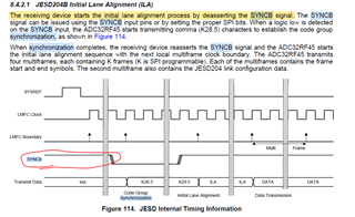
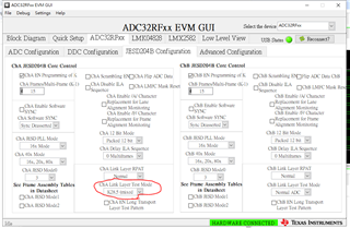
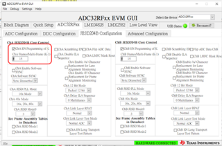
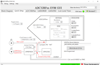
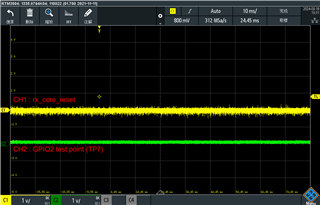
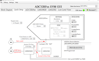
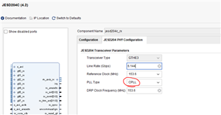
I used ADC32RF45 EVM and FPGA sent SYNC to ADC . but I measured ADC'output data which didn't show K-code(28.5).
Do you have any idea? this problem have been taken me lots of time.
thank you.
Hi Sir :
I used ADC32RF45 EVM and FPGA sent SYNC to ADC . but I measured ADC'output data which didn't show K-code(28.5).
Do you have any idea? this problem have been taken me lots of time.
thank you.