This thread has been locked.

If you have a related question, please click the "Ask a related question" button in the top right corner. The newly created question will be automatically linked to this question.

DAC7718: DAC7718SPAG Power Up and Reset Anomaly

Part Number: DAC7718

Hello,

I am using the DAC7718SPAG on a board i have designed.  I am seeing the VOUT-X lines go to about 9V after I release the reset line.   This seems

strange as I expected them to remain at 0V.

I HAVE THE FOLLOWING ADDITIONAL INFO FOR THIS:

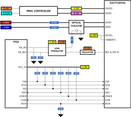
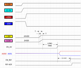
RSTSEL = USB#/BTC = IOVDD = 1.8V

IOVDD = 1.8V (powered on first)

DVDD = 3.3V (powered on second)

AVDD = +15V (powered on third and simultaneous with) ... AVSS = -15V

REF-A = REF-B = 4.096V (powered on last)

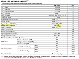
According to the data sheet, this should configure the DAC as follows: 

Dual-Supply

Twos Complement (input format)

VOUT = 0V (after RST# goes high)

However, I should mention that AVDD/AVSS/REF-A/B are all enabled by an FPGA.  At this point, I am programming the FPGA

over JTAG.  Once programmed, and once a jumper is manually removed, the logic automatically enables AVDD and AVSS, then

waits about 10 msec and enables REF-A / REF-B.  So, there is a "human speed" time delay from IOVDD & DVDD to those three supplies

coming up.

Does that signal a red flag?  The data sheet specifies supply sequencing but says nothing about required delay time between the

supplies.

Any insights and thoughts are appreciated.  Thanks!

  • I'm a bit confused ... in this thread:

    https://e2e.ti.com/support/data-converters-group/data-converters/f/data-converters-forum/933728/dac7718-offset-and-power-on-reset-issue

    ... Akhilesh K asks David Park (thread starter) to validate the proper power sequence and repeats the datasheet power sequence:  IOVDD -> DVDD -> AVDD/AVSS -> REF

    However, David Park indicates:   IOVDD->AVDD->AVSS->DVDD-> REF  (a DIFFERENT sequence from the data sheet)

    But then Akhilesh K acknowledges that his power up sequence is correct.  Is there a mistake in the data sheet?  Which power-up sequence

    is correct?  Perhaps there is a difference between DAC7718 and DAC7718SPAG?

  • Hi Dana, 

    Follow the datasheet recommendation of IOVDD/DVDD > AVDD/AVSS > REF. Maybe Akhilesh misread the response from David because I see that Akhilesh quoted the datasheet in the response directly before. 

    There should not be an issue with your human delay from enabling AVDD/AVSS & REF. The supplies basically supply the analog circuitry, but the digital circuitry should have initialized fine due to you enabling IOVDD & DVDD first. Can you read back the data register and check the data that is there?

    Can you also share a schematic of your board? Do you have any load connected to the output?

    Best,

    Katlynne Jones

  • Katlynne,

    Thanks for the informative response!

    Here is an image of my schematic (it is spread across multiple pages, and is hard to follow, so I encapsulated it with

    Visio.  Besides, I can use this myself later)  Slight smile

    I use pulldowns on the AVDD/AVSS enable and the REF enable to ensure not enabled to account for the FPGA not being programmed.

    I have 0.5-Ohm resistors in the +/-15V path to avoid a sudden jump in voltage on the AVDD/AVSS bypass caps (not shown).  The images look

    fuzzy to me. If you can't see them properly, let me know and I will e-mail them to you.  I didn't seem to be able to attach files.

    Here is a timing diagram of the power-up (there is 10 msec between EN_AV and EN_REF).

    Maybe something in the above stands out as a problem?  I have gone over it multiple times and can't quite seem to see an issue.

    I should note that IOVDD and DVDD START TO COME UP at the same time.  However, IOVDD reaches its full value (1.8V)

    in T msec, whereas DVDD reaches its full value (3.3V) in 2T msec.  I believe this satisfies the part's requirements (IOVDD at

    the same time or before DVDD).

    The DAC analog outputs are loaded with a 49.9KOhm to GND and also driving the non-inverting input

    of an op-amp buffer/follower circuit (high-Z in parallel with 49.9K).  They also have a 0.1uF cap on them.

    When I finally release RST#, the analog outputs rise to about 9.00V, but then seem to slowly decline.  I'm expecting

    them to be fixed at 0V until I start exercising the SPI Bus.  I have diagnostic code written for the FPGA to run the SPI

    interface (driven by manual switch settings) but have not yet got around to exercising that.  The difficulty is that the DAC

    outputs are driving a motor control which is getting set at near max level and I'm getting huge current on 15V and -15V. 

    So, there may be another problem, but whatever that is is getting a bit in the way of this.  I just want to validate that the

    DAC7718 end of things is sound. 

    Sorry for all the text.  I'm trying to give a complete picture so you aren't flailing with all kinds of questions.  Thanks again for any feedback.

  • Another question comes to mind.  I could not absolutely peg this down from the datasheet.  

    If I give the DAC7718:  REF=4.096V, AVDD=15V, AVSS=-15V, USB#/BTC= OVDD, GAIN=6

    Then I SHOULD HAVE:

    OUTPUT RANGE:  -12.288V to + 12.288V

    INPUT FORMAT:  2s complement

    Since this is a 12-bit DAC, this makes the AMPLITUDE effectively 11-bit, right?  (one bit being "spent" on the sign)

    This means that writing a 0111 1111 1111 to a DAC channel should make the output go to near +12.288V (max positive amplitude)

    writing a 1000 0000 0000 to a DAC channel should make the output go to -12.288V (max negative amplitude)

    But if I give the DAC7718:  REF=1.024V, AVDD=15V, AVSS=0V, USB#/BTC=GND, GAIN=4

    Then I SHOULD HAVE:

    OUTPUT RANGE: 0V to 4.096V

    INPUT FORMAT:  straight binary

    Since there is no sign bit, then I truly have 12-bit for the AMPLITUDE.

    If I write a 0111 1111 1111 to a DAC channel, that would make the output go to 2.048V (1/2 of max amplitude)

    Is this interpretation of the bits correct for these two contrasted setups?

  • Hi Dana, 

    I can see your images clearly when I click on them. Thanks for sharing.

    One concern that I did not catch in your original post, the max limit of the reference is DVDD, so your 5V reference is greater than your 3.3V DVDD. Is it possible to connect DVDD to 5V and see if the issue resolves? 

    About your second question, yes the resolution for the amplitude would effectively be 11bits. In 2's compliment 0111 1111 1111 (0x7FF) will give the positive full-scale output, 0000 0000 0000 (0x000) will give the zero-scale output (0V), and 1000 0000 0000 (0x800) will give the negative full-scale output. 

    In straight binary, 0111 1111 1111 (0x7FF) actually gives mid-scale - 1LSB. 

    This table from the datasheet pretty much confirms your understanding. Just replace with your intended gain setting. 

    Best,

    Katlynne Jones

  • Ok, thanks for that response.  I missed that.  Uggh.

    I am working from home today, but will see what I can do with the reference tomorrow as I am going in to the office. Actually, I did not show that reference

    well.  The reference is POWERED BY 5V, but is actually 4.096V.  This is still above the 3.3V DVDD.  So I have to figure that out.  I have the gain set at 6, so

    my output range is (supposed to be) 24.576 (-12.288 to +12.288).  Luckily my FUNCTIONAL range is -9.00V to +9.00V.  I was planning on implementing

    out-of-range safety into the FPGA code by not sending anything that would have an amplitude greater than 9V.  But I think I will have to go the better

    route now (from safety perspective) and set the reference at 3.0V.  I just lose that nice bit pattern associated with 4.096V (2^12 = 4096).  Oh, well.

    Thanks again!  I'll let you know how it goes.  I really do appreciate the feedback.

    Will having DVDD at 3.3V and REF at 4.096V cause physical damage to the device?  This has already happened.

  • Hi Dana, 

    I doubt it has caused any catastrophic damage to the device. Operating the device in that condition consistently over a long period of time could degrade the internal components of the device and cause reduced performance, but that is not likely to have happened with the few times you have operated the device so far. 

    Best,

    Katlynne 

  • Katlynne,

    I got pulled off onto other duties and returned to this again today.  I want to thank you for taking the time and for getting me past

    my hurdle.  I ended up replacing my reference with 3.0V and when I release from reset, the DAC outputs remain at 0V as I was

    expecting in the first place.  Your response has resolved my issue.  Thanks again!

  • Hi Dana, 

    Great to hear and thanks for following up! Please let me know if you run into any other issues. 

    Best,

    Katlynne Jones