This thread has been locked.

If you have a related question, please click the "Ask a related question" button in the top right corner. The newly created question will be automatically linked to this question.

DAC7718: Offset and power-on reset issue

Part Number: DAC7718

Hi,

There is wrong offset and abnormal output in power-on/off as below description.

1. OFFSET_A is around 2.6V at 000h with dual supply. When it's 800h, OFFSET_A was 0V.

2. Output is around -5V with RSTSEL->IOVDD, /USB/BTC ->IOVDD

Setting is

Configuration: 858h

Monitor: 000h

GPIO: E00h

Offset DAC-A: 000h

Offset DAC-B: 000h

SPI MODE: 000h

Read back is already done.

Output is 2.6V with 800h for 0V and 7.6V with 840h for 5V.

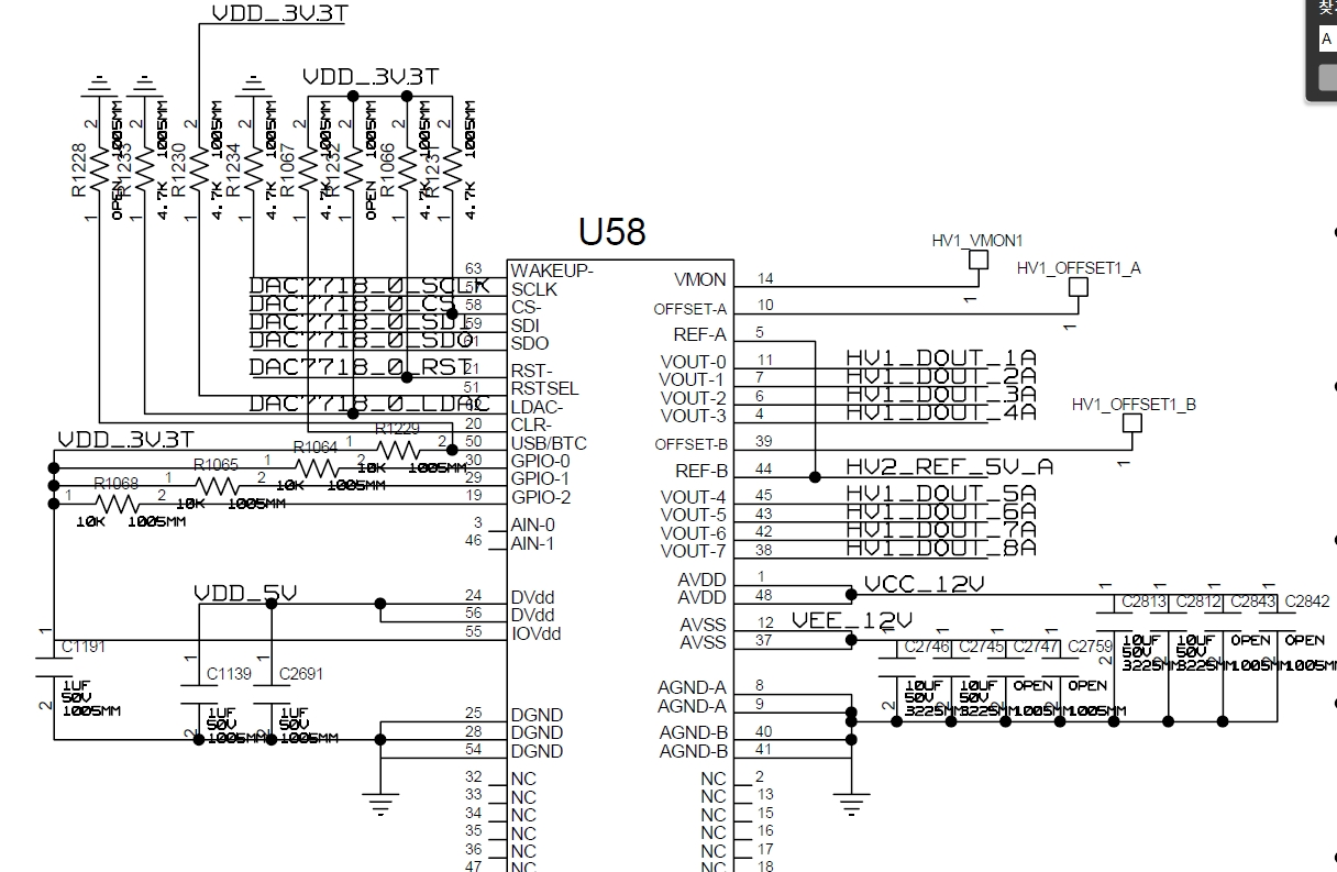
Schematic is as below.

  • Hi David, my colleague Akhilesh will help you on Monday.  

    Thanks,

    Paul

  • Hi David,

    Couple of questions:

    1. What is the reference input, is it 5V or 2.5V, I cannot get that info from schematics. Please make sure that reference input is less than or equal to DVDD.

    2. As per your schematics, your data is two's compliment right?

    3. Also after a power on RESET, whats the value of Offset DAC register? It should be 0x19A

    4. Make sure that Offset DAC output is not connected to nay kind of load.

    Please verify these and let me know.

    Regards,

    AK

  • Hi AK,

    1. 5V. you can see it in the schematic

    2. yes

    3. it's 0x800 so it's weird.

    4. don't connected any load

  • Hi David,

    Thanks for confirming the queries.

    Can you tell me the power up sequence? Which supply comes first and which comes last?

    Can you take scope shot of the power up with respect to AVDD, AVSS, IOVDD, REF and DVDD?

    For proper power-on initialization of the device, IOVDD and the digital pins must be applied before or at the same time as DVDD. If possible, it is preferred that IOVDD and DVDD can be connected together in order to simplify the supply sequencing requirements. Pull-up resistors should go to either supply. AVDD should be applied after the digital supplies (IOVDD and DVDD) and digital initialization pins (LDAC, CLR, RST, CS, and RSTSEL). AVSS can be applied at the same time as or after AVDD. The REF-x pins must be applied last.

    Regards,

    AK

  • Hi AK,

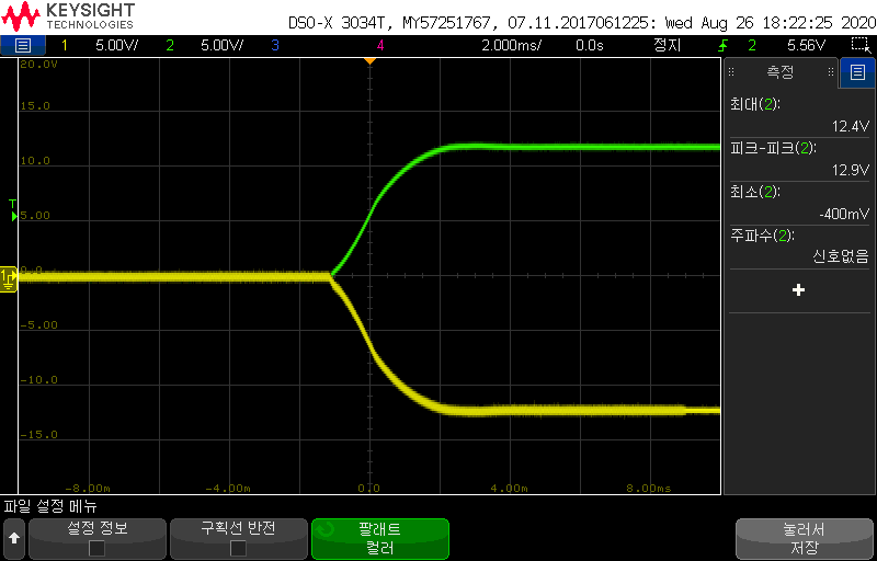
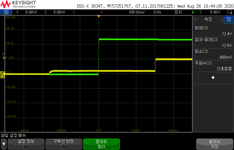
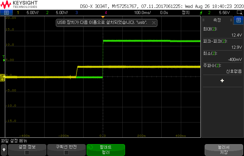
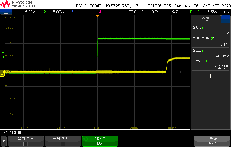
    It's IOVDD->AVDD->AVSS->DVDD->REF

    AVDD: Green, AVSS:Yellow

    AVDD:Green, DVDD:Yellow

    AVDD: Green, IOVDD: Yellow

    AVDD: Green, REF: Yellow

  • Hi,

    Power up sequence is spot on and looks clean, I don't see any issues.

    Can you try with another device to check, if the same problem persists? 

    Regards,

    AK