This thread has been locked.

If you have a related question, please click the "Ask a related question" button in the top right corner. The newly created question will be automatically linked to this question.

DAC39J84: JESD routing - Is the data in the IBIS file required

Part Number: DAC39J84


hello,

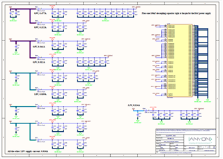
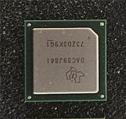
Is the data in the IBIS file required to match net length when running the JESD interface at 10 or 12Ghz? or is it sufficient to equalize just the traces to the DAC39J84 device from an FMC connector?

(ie will the JESD protocol be able to lock on without any lane errors)?

thanks again

Matthew

  • Hi Matthew,

    There is no length match requirement between different serdes lanes. In JESD204B, any lane mismatch is accounted for by use of an elastic buffer during link bringup in a stage called ILAS (initial lane alignment sequence). The DAC (the jesd receiver) has a register for setting the release buffer delay (RBD). A larger value will increase link latency but allow for longer mismatch between any lanes of a link. A shorter value is useful when low latency is required. This would be the only time length matching across jesd lanes would be suggested.

    Thanks, Chase

  • What else would cause lane errors on different boards?

  • btw, registers:

    0x4b = 1f00

    0x4c = 1f07

    which should be the largest value possible.

  • The lane errors reported are always random...

    Register 0x64 - 0x6a report 0x3 or 0x9 or 0xb

    some boards work reliably, others give these lane errors.  We've replaced the DAC, checked the soldering, checked the connections...  no sure what else to check

  • Hi Matthew,

    Can you try to reset the jesd core of the DAC after data is being sent by the FPGA? I suspect the fifo errors are not being reset by the dac jesd core reset while data is actively sent by the fpga. In the datasheet it shows to write to clear these registers but in the past we have seen issues with doing just that alone for some reason. To fix, usually just resetting the jesd link from the dac by writing init_state to 0xF and jesd_reset_n to 0 and then writing back init_state as 0x0 and jesd_reset_n as 1. Then clear all alarms by wriiting value 0x0 into the alarm registers. This should provide you with accurate status of each alarm.

    Thanks, Chase 

  • Hi Chase

    This is the procedure that we use.... First on a good/working board:

    -------------------------------------------------------------------------------

    Write 0xFF1E to register 0x4A

    set-up DAC configuration registers

    write 0xFF01 to register 0x4A

    read error registers


    Clear alarm Status by writing 0x0000 to the above registers

    read error registers again

    Enable TXEN  and there is an analog output

    -------------------------------------------------------------------------

    On the none functioning boards (same procedure - same fpga - same code)

    Write 0xFF1E to register 0x4A

    set-up DAC configuration registers

    write 0xFF01 to register 0x4A

    read error registers

    Clear alarm Status by writing 0x0000 to the above registers

    read error registers again

    Enable TXEN  and there is no analog output

    Any clue or other suggestions?

    thanks again

    Matthew

  • Matthew, 

    Is it possible to cut the serdes by 2 and check at a lower serdes rate, first on a functional board to verify the serdes link is ok and then try using a failing board?

    Chase

  • Hi Chase,

    We tried this before, and the working boards had no issues.  The boards that didn't work failed.  Is there something in particular that you want us to look at after we make that mod?

    Matthew

  • No, every board shop is different so that test was just to check if their qc was bad and the signal integrity was ok at lower rate. 

  • Matthew,

    During the sequence you mentioned above, there is an active data flow from the fpga under all conditions? This would certainly cause empty fifo errors if inactive in some of the cases. I am having to think about things that are changing when you shift from one setup to the other now which is difficult.

    Do you have more than one DAC on a single board? Can you draw a very basic block diagram of your system or share a portion of your schematics so I can think of anything else to check or try?

    Chase

  • 1- the original DAC chips that we received were from Digikey.  Out of the 40 boards that were manufactured, only 15 work and all the others have this lane error issue.  We just received another batch of chips directly from TI this morning, so we will probably rework 3-5 boards and see if that makes a difference.

    2- yes, there is only 1 DAC39j84 on this board.  It is a small FMC card, with the fmc connector on one end, the DAC in the middle, and SMA connectors on the other end.  There is some support circuitry (Power, LMK clock gen, etc) on this board as well.  The boards were manufactured by TTM which we always had good experience with.

    3- Part of the sch below

    Matt

  • Hi Matt,

    Any update on this after the reworked boards?

  • Hi Chase,

    1- They installed a new X-ray machine this weekend, so we were looking at the pcb layers, and could not see any differences between the good and bad boards.

    2- We received the new chips directly from TI, but haven't installed them because we need some clarification on what was shipped.  Do you know what the markings on the chip mean?  What is the Date code or batch number?  These have the exact same labelling as the ones that are not working. so it doesn't seem like it is a different batch of chips.  

    Attached is a pic of the new chip.  What do these numbers mean and what is the batch/date code?

    Matt

  • Matt,

    I don't know myself what the markings mean. This would take some time to find out probably but I will start that process. You have confirmed that the marking on the functioning devices are different than the non-functional devices? Can you share a picture of the functioning devices also? This might be of interest for helping distinguish, etc.

    Thanks, Chase

  • Hi Chase,

    Currently, the working boards are installed on a quantum computer, I will check with that team if we can pull one of those cards from the backplane.  I'll let you know as soon as I get info. 

    The other thing I noticed is that the heatsink on top of the chip is causing temperature variations during reflow.  Do you have any documents or procedures on how to reflow these parts reliably?  Do they require a lower temp but higher soak time?

    Matthew

  • Hi Matthew,

    We recommend a JEDEC standard Pb-free reflow profile. These are MSL3 260C peak devices. Please review the following app note: https://www.ti.com/lit/an/spraby1a/spraby1a.pdf 

    Best regards,

    Drew

  • Hi Chase,

    1- do you have any idea what the marking on the TI chip means ?? (Can you escalate this issue)?

    2- The boards which are working have the same markings

    3- can you fix all the errors in your datasheet.  There is nothing more frustrating that getting bad information from TI.  Register mapping in your pdf (latest version on your webiste is wrong).  As an example, register config100 is at address 065h?  i dont think so... The entire table is shifted off

    4- Can I get a proper temp spec for this part?  If we reduce the oven temp but leave the dwell time longer, we get a better success rate.  50% drops to 40%.

    5- Can I also get reliability data on this chip?  We are seriously thinking about remove this from our design,   We cant seem to get proper support for these devices.

    Matthew

  • Hi Matthew,

    1) For the “markings” I see a TI logo, the part #, and a lot trace code.  No surprises or concerns here.  When I googled ‘ti lot trace code’ I found this,

    What is a Lot Trace Code (LTC) and where can I locate it?

    The Lot Trace Code is a 7-digit code marked on each TI device representing a single lot processed through one controlled assembly flow. It might appear in a single line or double line. The code is located with the markings on the top side of the device.

    Part marking example of LTC can be found using the part marking lookup tool

    2) ok, thank you for verifying.

    3) Yes, we are working on the datasheet fixes, thank you for bringing this to our attention. I put in a ticket today to have this updated. We apologize for the confusion.

    4) Unfortunately, we do not have a spec around the temp sensor, we can’t guarantee anything more than what the datasheet says. There is a note on accuracy in the datasheet:

    >In order for the process described above to operate properly, the serial port read from config6 must be done with an SCLK period of at least 1 μs. If this is not satisfied the temperature sensor accuracy is greatly reduced.

    5)  Reliability data is all on ti.com product page – look at the quality/reliability section.

    https://www.ti.com/quality-reliability-packaging-download/report?opn=DAC39J84IAAV

    If you would like, you can return a few of the affected parts and TI’s FQE (that’s field quality engineering team) or DCC’s sustaining team can support the return, re-ball, and re-test on ATE to validate the device.

    If you suspect this is an assembly issues, we are happy to look at your layout to understand more here. It would be good to provide the fabrication notes as well.

    Regards,

    Rob