This thread has been locked.

If you have a related question, please click the "Ask a related question" button in the top right corner. The newly created question will be automatically linked to this question.

ADC3683: How to realize simultaneous sampling between two different ADC3683s without using Decimation?

Part Number: ADC3683


Hi Teams,

Hope you are doing well.

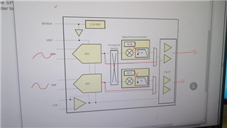
How to realize simultaneous sampling between two different ADC3683s without using Decimation? The input signals for two ADC3683s have been trimmed simultaneous.

Looking forward to your reply.

BRs,

Marsh

  • Hi Marsh,

    Are you saying, the customer would like to sample two different devices at the same time?

    Are they planning to sum the digital data together or do interleaving?

    Either way, they will need to create an analog input network that connects all the analog input together.

    They will need to do the same on the clock if they plan to sum, if they plan to interleave, then you need to have a phase shifter between each clock/device.

    Thanks,

    Rob

  • Hi Rob,

    Thanks for the help. Yes, Customer is trying to sample two different devices at the same time. The inputs are from the POWER DIVIDER, so their are literally same. And outputs will do interleaving.

    The customer's question is how to guarantee two ADC3683s to do the sampling simultaneously? 

    Either way, they will need to create an analog input network that connects all the analog input together.

    For the saying above, POWER DIVIDER is used for input.

    They will need to do the same on the clock if they plan to sum, if they plan to interleave, then you need to have a phase shifter between each clock/device.

    For the saying above, do you mean that what customer need to do is to apply the required inputs and clocks, the ADC3683s will work. No any other configuration needed? Like some other sync pin for synchronization?

    BRs,

    Marsh

  • Marsh,

    The clock inputs must be the same length from the common clock source. This will guarantee the two ADC are sampling at the exact same instance. The SYNC pin is not needed since there are no internal clock dividers active in bypass mode. However, I would highly suggest to connect the SYNC pin in the event that the customer would like to evaluate using a decimation mode, which is most common for these newer products.

    Thanks, Chase

  • Hi Marsh,

    Some of you comments are not correct.

    Please look at this older article to understand the differences between summation of ADCs and interleaving ADCs.

    All clock and analog input need to originate from the one source and be length matched, with the exception that for interleaving, you need to phase shift the clocks between each ADC, as the link describes below.

    www.analog.com/.../multichannel-a-d-converters.html

    Regards,

    Rob

  • Hi Rob,

    Thank you so much for the reply. There's a little bit difference between this appnote & real usage.

    We didn't use cross two channels. We are using 2*ADC3683s sampling signals independently. There are 4 channels in total between the two 3683s. Each channel samples the same sine wave with the same phase. The result of the testing is that the waveform phases of the two 3683 outputs will occasionally be out of sync. Because we haven't seen any nco and downsampling modes inside the ADC3683, the sync pin mentioned in the manual cannot be used as a synchronization pin to synchronize the chip. So, in this case, our question is does ADC3683 support synchronization, and if so, how to ensure that the output is synchronized?

    Looking forward to your reply, thank you!

    BRs

    Marsh

  • Hi ROB,

    Could you kindly help to review & support this request?

    BRs,

    Marsh

  • Marsh, I just talked with Rob about this so I will post on his behalf.

    We are still unsure of the system design. For instance, in the above messages, you are mentioning inputs are from a power divider. Is this the analog input channels or the clock inputs?

    If the clock inputs are aligned, the ADC is guaranteed to store the sample at the exact same instance so long as the clock traces are the exact same. The only reason the data would not be aligned at the FPGA under these conditions above would be something related to the DCLKIN phase between the devices. How is the DCLKIN, DCLK, and FCLK routed? It is critical that the FPGA meets timing on all of these inputs.

    We also don't fully understand what is meant by the signals will occasionally be out of sync. Can you specify more on occasionally and also share images for the good and bad captures?

    Thanks, Chase