This thread has been locked.

If you have a related question, please click the "Ask a related question" button in the top right corner. The newly created question will be automatically linked to this question.

ADS8910B: RVS Pin not responding

Part Number: ADS8910B
Other Parts Discussed in Thread: THS4551

Hello,

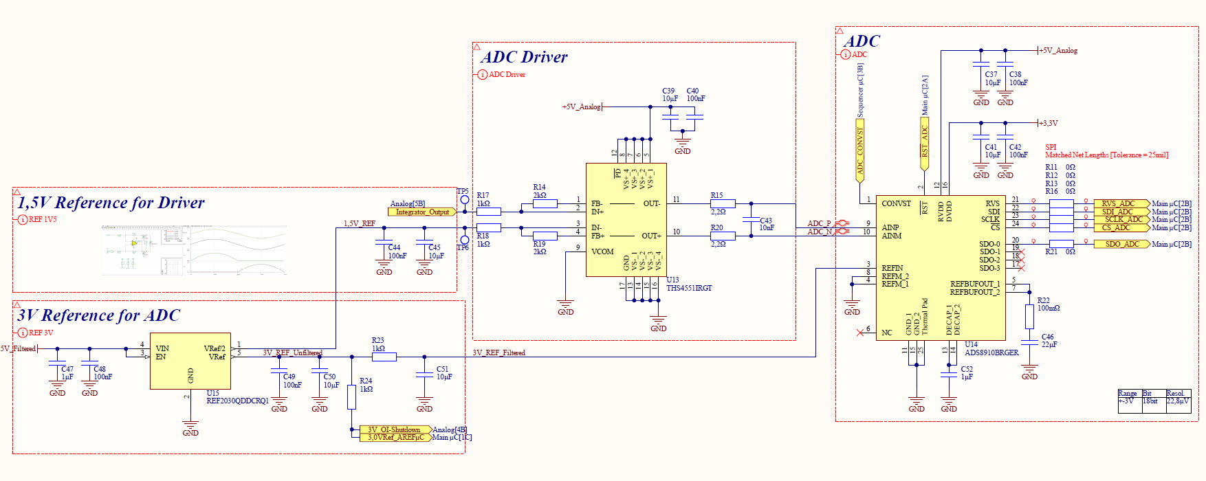
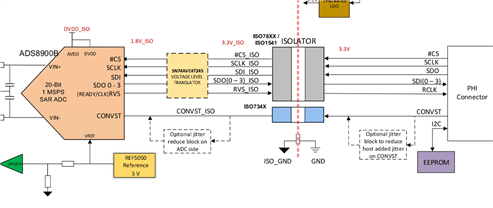
we are currently working on some  prototypes using the ADS8910B and the STMF730 and after a few weeks several of our Boards ADS8910B's aren't responding the way they should to the CNVST Signal they're receiving.

The microcontrollers and the digital part of the ADS8910 are supplied with 3V3, the analog part of the adc is supplied with 5V

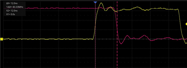
The ADS8910B gets its CNVST from another ST µC which only does the timing, the HIGH-level of the CNVST Signal (3V3) sent is about 50ns wide, which is well above the minimum of 30ns specified in the datasheet and worked without a problem so far (and still works on the remaining functional boards).

The expected behaviour is that if the Chip Select on SPI is HIGH, RVS should mirror the internal state of the ADC and if Chip Select is low, it should also go low.

We use this behaviour to trigger an interrupt on the F7 and get the measurement data via SPI (in zone 2), therefore the RVS is on an GPIO mapped as falling edge interrupt, without any pull-ups or pull-downs, neither hardware, nor software enabled internal ones.

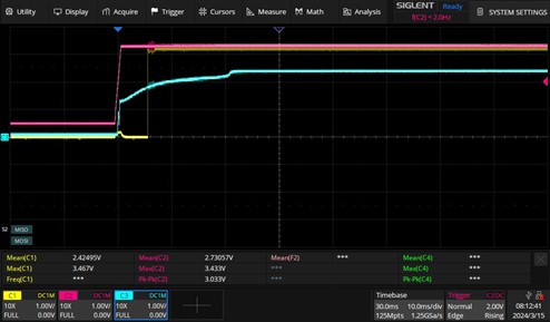
But for the "supposedly dead" ADS8910B's it's that even when there's no CNVST trigger and the Chip select is high, the RVS remains low - some 200mV measured with a scope which remain constant, there's no swinging or anything.

Since the absolute maximum currents on the digital interface of the ADS8910B are quite high (130mA) and the supplied voltages to both ADC and µC are the same i don't think the ADC's died due to overcurrent.

Besides the F7 SPI interface still works fine and there's no series resistor, so it should have died as well if it was ESD.

Oh and the current draw is still normal as well, not too much heat on the ADC's either.

Is there anything besides Chip Select and the internal State of the ADS8910B that affects the RVS?

Are the ADC's dead if there is no response on the RVS?

I'll gladly provide more information if needed.

Greetings,

Michael

  • Thanks, Michael. 

    Which data read protocol are you using in the ADS8910B? We can look further into this next week.

    Regards,

    Ryan

  • Hi Ryan,

    at the moment we are not actively changing it, so it should be the SPI-00-S Protocol that's used after the ADS8910B  powers up.

    Regards,

    Michael

  • Hi Michael,

    The absolute max current rating of ±130 mA only applies to the analog inputs, not digital I/O. I believe the IOVDD supply only powers the output cells and level translators, and you should not see more than a few mA at full clock speed. Can you check the IOVDD current after power up for a failing unit?

    It's still a possibility that the IC was damaged somehow. If you replace the IC on a failed board, does that resolve the issue? Can you provide a schematic as well so we can review everything that is connected to the ADC and how it's powered?

    Regards,

    Ryan

  • Hi Ryan,

    thanks for the quick response.

    You are absolutely right, the 130mA only apply to the analog inputs, i misread that.

    We have 1 board with way too much current draw on the 5V side, but the other 2 "broken" boards don't have a much higher current on 3V3 or 5V. I will measure the currents on the ADS8910B input seperately and post an update on that.

    Here's the schematic for the ADC:

    As well as a snippet from the simulation for the THS4551 which we use to drive the ads8910B:

    And here's a scope shot of the working board with CNVST (yellow) to RVS (red), the non-working boards simply don't respond, the CNVST-Pulse there is identical though.

    1V/div 10ns/div

    Regards,

    Michael

  • Hi Ryan,

    i just measured the IOVDD (DVDD) and across all defective boards the current was 0, not even some µA. Looks like they died completely on the digital side :/

    The analog input drew some 3mA

  • Thanks, Michael.

    One issue I found with the schematic is the output common-mode voltage of the THS4551. The ADS8910B requires an input common-mode voltage equal to VREF/2 ± 100 mV. Currently, you have connected the amplifier's VOCM pin to GND with a single-ended to differential circuit. This is causing the common-mode voltage to the ADC to exceed these limits:

    Regards,

    Ryan

  • Thanks Ryan,

    i completely forgot to change that.

    Can this also be the reason why the digital side seems to have died?

    Regards,

    Michael

  • Hi Michael,

    I would not assume so. The input common-mode is a requirement for the sample-and-hold circuit to perform properly. Violating this usually results in linearity performance degradation.

    Regards,

    Ryan

  • Hi Ryan,

    so yesterday the last ADS8910B stopped working on the digital side.

    I am measuring 2.85V on the DECAP pins and 2.99V on the Refbufout, so i think the internal Supply still kinda works. (Sadly i didn't measure the voltage on those Pins before they gave up on me and therefore i have no reference)

    Can it cause problems when the ADC is still in Reset-State after bootup and there's already a signal on the analog input?

    When the Host controller enables the ADC, there's already about 2V on one of the inputs:

    Red: 3.3V Rail

    Yellow: RST Pin of the ADS8910B

    Blue: Signal on AIN_P

    Or is it more likely that an event on the Digital side killed the RVS/SPI interface?

    The only thing attached to those pins would be the STM32F730's SPI4 Pins, and that chip is on the same GND and 3.3V rail.

    I've seen in the TIDA refdesign schematics an isolator is used and the digital IO voltage is reduced to 1V8 on the adc side, is this necessary here as well? For both the 8910B and the 8900B, from the values in the datasheet i would not deem it necessary.

    But until now i never had the need for SPI isolators and thus i'm not really knowledgable about when and how to best use them.

    Last but not least: is there anything besides the RVS behaviour and SPI that i could test from the outside to determine what exactly died on the inside ? (and how)

    Thank you for the support!

    Michael

  • Hello Michael,

    In mode ADCs, the analog inputs can be driven as long as the analog supply voltage has ramped. In the ADS8910B, the Abs. Max Ratings table refers the analog inputs to VREF, so I would also check that the REF5050 output has at least started ramping before the analog input voltage. If that's the case, then I would not expect any damage while the device is held in RESET state after startup.

    Also, you cannot use a 5-V reference (REF5050) with a 3.3-V supply. Your original schematic showed 5-V supply, but the block diagram above shorted AVDD and DVDD. REFIN is limited to RVDD-0.3V, which might explain why the REFBUFOUT is measuring 2.99V.

    Regards,

    Ryan