This thread has been locked.

If you have a related question, please click the "Ask a related question" button in the top right corner. The newly created question will be automatically linked to this question.

AMC1204: Clarification on accumulator

Part Number: AMC1204


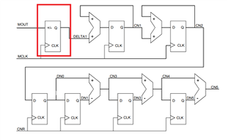
Hi guys, I am taking a look to SBAA094 and I don't understand behavior of sinc filter on VHDL code about input bitstream:

- ...000000... means -Vref
- ...111111... means +Vref
- ...0101010 ... means 0V

At reset DELTA1 is set to 0x00 (let's use hex notation), but while MOUT = 1, DELTA1 will be incremented.
No way to decrease DELTA1?

M=1 then DELTA = DELTA+1

Shouldn't be M=0 then DELTA = DELTA-1?

Thanks.

  • Hi Michele,

    Why do you want to decrement DELTA1? The code is based off of figure 13 which should be consistent. You could always copy the code and alter it for it to best fit your application if there is a reason you need to decrease DELTA1. Please let me know.

    Best regards,
    Eva

  • Sorry Eva, many years have passed since I don't use VHDL, I am still trying to simulate module...

    First of all I'm confused about "+/-" input of FF1...

    It looks such a flip-flop, then I expect DELTA1 as std_logic but taking a look to VHDL code it seems to be an up-counter due to std_logic_vector.

    Bus width is 25 bits so is it a 25 bit sinc3 filter or is it a 24 bit filter where I need to keep additional bit?

    On schematic I can see only 2 integrator blocks while 3 differentiator blocks, shouldn't it be paired, so 3 and 3?

  • Hi Michele,

    I wasn't able to see the picture you inserted, but I'm assuming it's the one I'm posting below.

    In the picture above, the block in the red is acting as the 1st integrator.  Since the output of a modulator is only '0' or '1' the integrator effectively just accumulates when MOUT = 1, and doesn't change when MOUT = '0'. 

    The bus width is 25 because of the gain of the filter plus the original 1 bit input (MOUT).  The table below shows the output size based on the decimation ratio.

  • Mmh... I made a simulation, I don't know where I am wrong...

    I created SDO signal simulating modulator output, sck is base clock while sck4 is output clock for decimator.
    First part is positive slope where SDO starts from 00000000... to ...11111111 (figure 3 of SBAA094), then back again to 00000.

    I expect CN5 starts from 0000, increases up to a positive value (end of positive slope), then going back to 0000.

    Here code I used:

    -- sinc3 vhdl code from SBAA094
    
    
    library IEEE;
    use IEEE.std_logic_1164.all;
    use IEEE.std_logic_unsigned.all;


    entity FLT is


    port(RESN, MOUT, MCLK, CNR : in std_logic;
                           CN5 : out std_logic_vector(4 downto 0)
    );
    
    end FLT;
    
    
    architecture RTL of FLT is
     signal DN0, DN1, DN3, DN5 : std_logic_vector(4 downto 0);
     signal CN1, CN2, CN3, CN4 : std_logic_vector(4 downto 0);
     signal DELTA1 : std_logic_vector(4 downto 0);
    
     begin
     process(MCLK, RESn)
        begin
           if RESn = '0' then
              DELTA1 <= (others => '0');
    
           elsif MCLK'event and MCLK = '1' then
     
              if MOUT = '1' then
                 DELTA1 <= DELTA1 + 1;
              end if;
           end if;
        end process;


     process(RESN, MCLK)
        begin
           if RESN = '0' then
              CN1 <= (others => '0');
              CN2 <= (others => '0');
           elsif MCLK'event and MCLK = '1' then
              CN1 <= CN1 + DELTA1;
              CN2 <= CN2 + CN1;
           end if;
        end process;


    process(RESN, CNR)
       begin
          if RESN = '0' then
             DN0 <= (others => '0');
             DN1 <= (others => '0');
             DN3 <= (others => '0');
             DN5 <= (others => '0');
          elsif CNR'event and CNR = '1' then
             DN0 <= CN2;
             DN1 <= DN0;
             DN3 <= CN3;
             DN5 <= CN4;
          end if;
       end process;
     
       CN3 <= DN0 - DN1;
       CN4 <= CN3 - DN3;
       CN5 <= CN4 - DN5;
    end RTL;

    library IEEE;
    use IEEE.STD_LOGIC_1164.ALL;
    use ieee.numeric_std.all;
    
    -- per le funzioni di output su console
    use STD.textio.all;                     -- basic I/O
    use IEEE.std_logic_textio.all;          -- I/O for logic types
    
    
    entity sinc_filter is
    end sinc_filter;
    
    architecture Behavioral of sinc_filter is


    signal sck, sck4 : std_logic; -- clock signals: sck = clock signal from modulator, sck4 = clock signal for output sampling frequency
    signal SDO :std_logic; -- output signal from modulator
    signal reset : std_logic; -- reset signal
    signal CN5 : std_logic_vector(4 downto 0); -- sinc3 output


    -- for debug
    constant DataWidth : integer := 6; -- larghezza in bit del bus
    signal a_slv : std_logic_vector((DataWidth-1) downto 0); -- se DataWidth  is 5 , allora a_slv va da 4 a 0 (5 bit)
    signal sck2 :std_logic;
    signal w : std_logic;
    signal bi : std_logic_vector((DataWidth-1) downto 0);


    -- sinc3 filter
    component FLT is
    port(RESN, MOUT, MCLK, CNR : in std_logic;
                           CN5 : out std_logic_vector(4 downto 0)
    );
    end component;


    begin
    -- qui assegno i segnali al componente in esame
    -- port map: component pin => testbench signal
    
    dut: FLT port map (
    
    RESN => reset,
    MOUT => SDO,
    MCLK => sck,
    CNR => sck4,
    CN5 => CN5
    
    
    );


    -- qui mi sembra io faccia partire dei processi concorrenti
    
    stim_proc: process
    begin        
       -- hold reset state at startup
         reset <= '0';
       wait for 1 ns;    
        reset <= '1';
       wait;
    end process;


    serialize_proc: process
    
    variable b : integer := 0; -- contatore di bit, b7, b6, b5, ....
    variable it : integer; -- contatore iterazioni
    
    
    begin
    -- inizializzo le variabili e i segnali
    sck <= '0';
    sck2 <= '0';
    sck4 <= '0';
    w <= '0';
    a_slv <= (others => '0'); -- inizializzo tutto a 0  
        wait for 1 ns;
    
    
    -- da adesso parte la simulazione vera e propria3
    
    for it in 0 to 22 loop
    b := (DataWidth); -- se io faccio partire b da 4, allora ho solo 4 passaggi nel ciclo while, se lo faccio partire da 5 allora ne ho 5
    
    while (b>0) loop
    bi <= std_logic_vector(to_unsigned(b-1, bi'length));
    SDO <= a_slv(b-1);
    
    wait for 10 ns;
    sck <= not(sck);
    
    if (sck = '1') then
    b := b-1;
    sck2 <= not(sck2);
    if (sck2 = '1') then
    sck4 <= not(sck4); -- sck4 period is 4 times sck period
    end if;
    end if;
    
    end loop;
    
    if (it < 20) then -- let's shift right to increase density of '1' in SDO signal
    a_slv <= a_slv((DataWidth-2) downto 0) & '1';
    end if;
    
    if (it > 34) then -- let's shift left to decrease density of '1' in SDO signal
    a_slv <= '0' & a_slv((DataWidth-1) downto 1) ;
    end if;
    
    w <= not(w); -- for debug purposes only
    
    end loop;


    wait;
    end process;


    end Behavioral;


  • Ok, increased bus width to 7 bits and CN5 output looks agree with expected results.