Hi,
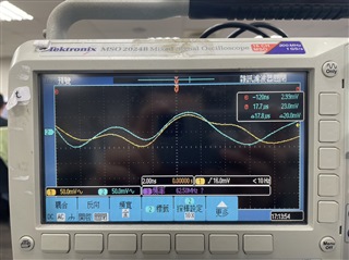
I am facing that there is no ADS4449 output signal at bit 1 and bit 2 while in test pattern mode. Please refer to the attachment for the two different phenomenon at ADS4449 output. Looks like there is no any signal applyed at bit 1 and 2, it's just the inphase common noise I think(or other possible reason). Which there is abvously a very clear P&N signal at other bits.
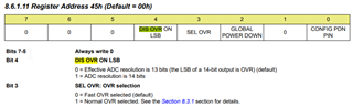
I have asked this issue last week, and also refer to the content, https://e2e.ti.com/support/data-converters-group/data-converters/f/data-converters-forum/1131411/ads4449-databit-fluctuation, by your kindly advise.
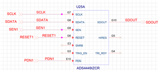
But its still got the issue after I checked all the registers mentioned in the above page.
I wonder if there is any other reasons could casuse the kind of issue.
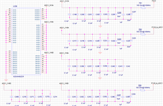
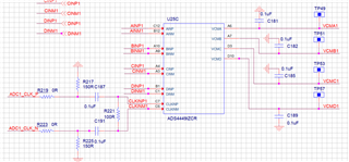
Attachments for your reference:
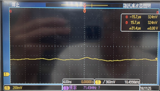
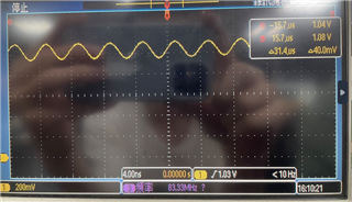
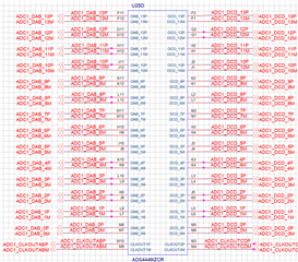
1. ADS4449 normal output(p&n), normal bits

2. ADS4449 unusual output(p&n), bit 1 & 2
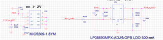
3. First stage

4. second stage
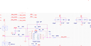
5. ADC input stage

Thank you for your assistance and look forward to hearing from you soon.