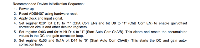
Hi Team,
Currently, ADS5407IZAYR part is used in our project.
Best Regards,
Sangam
This thread has been locked.
If you have a related question, please click the "Ask a related question" button in the top right corner. The newly created question will be automatically linked to this question.
Hi Team,
Currently, ADS5407IZAYR part is used in our project.
Best Regards,
Sangam
Sangam,
The CLKIN needs to be supplied in order for the clkouts to function.
Regards,
Geoff
Sangam,
On page 27 of the datasheet it is recommended that the device have a hardware reset after power up to all the internal digital blocks to their default conditions. Can you please verify this is what is being done at powerup?

Regards,
Geoff
Hi Geoff,
This recommendation has been taken care and followed, but no luck. Any other things needs to be done?
Best Regards,
Sangam
Sangam,
Outputs are LVDS and need to be terminated with 100Ω diff in order to switch. Are they properly terminated? If they are then I'll need to get an EVM and see what else needs to be setup.
Regards,
Geoff
Geoff,
Yes, Both LVDS Clock Outputs are terminated with 100Ω.
Best Regards,
Sangam
Sangam,
Can you give us the schematic section of the ADS and we'll work on getting an EVM setup next week to replicate the issue.
Regards,
Geoff
Geoff,
Could you please share your mail ID to send schematic section of the ADS.
Best Regards,
Sangam
Sangam,
We are looking into an EVM to check the issue you are seeing.
Regards,
Geoff
Hi Sangam,
What is the voltage level directly at the clock pins on the ADC?
Can you please verify that?
Regards,
Rob
Hi Sangam,
Could you also please verify that the output clock buffers have not been disabled via SPI?
D3 and D4 of Register 3A should be zero.
Best regards,
Drew
Hi Rob,
Voltage level directly at the clock pins on the ADC reading around 700mV.
Best Regards,
Sangam
Hi Drew,
Yes, output clock buffers have been enabled via SPI, but still no luck. However I believe output clock buffers are enabled by default.
And To enable clk buffers, D3 and D4 of Register 3A should be one not zero right??
Best Regards,
Sangam
Sangam,
Yes, that is correct. Just wanted to make sure they weren't accidentally getting set to 0 and powering down the clock buffers. (They should be 1 by default).
Regards,
Drew
Hi Sangam,
Is it possible for you to check the status of the ENABLE pin on the device? Is this pin pulled high?
Best regards,
Drew
Sangam,
Thank you for checking this. I think the next thing to check will be the schematic. Would you mind sharing that? My email is drewharrell@ti.com
Best regards,
Drew
Sangam,
I received it. I will report back with an update by the end of the week.
Best regards,
Drew
Hi Sangam,
Is this currently being seen on just one part? Is it possible to check other parts for the same occurrence?
Best regards,
Drew
Drew,
All five ADCs of the same part on-board are experiencing identical issues.
Best Regards,
Sangam
Hi Sangam,
Sorry for the delay, can you please send over our spi register writes for the ADC?
The schematic looks fine to us. Please ensure there is a termination resistor installed on the ADC clock outputs per your schematic. If so, are you using the FPGA termination resistors as well?
If you are seeing this on multiple ADCs, have you probed the ADC clock outputs directly with an oscope? Have you measured the DC common mode voltage on any of these clock outputs? Please let us know.
Thanks,
Rob
Hi Rob,
SPI register writes would looks like below,
Reg Value
0x00 0x0
0x01 0x8202
0x02 0x0780
0x03 0x4B18
0x1A 0x4B18
0x03 0x0B18
0x1A 0x0B18
0x0E 0x5554
0x0F 0x5010
0x3A 0x081B
0x66 0xFFFF
0x67 0xFFFF
We have used 100ohm Termination resistors at the FPGA end. We have measured DC common mode voltage for DACLK output as you can see in the attached image.

Best Regards,
Sangam
Hi Sangam,
Thank you for sending this over. I noticed the data for register 0x0F is not default. The internal LVDS termination is getting changed. Is this intended? Does the output clock come up if you leave this at default setting?
Best regards,
Drew
Hi Sangam,
Also, could you try writing 0xD2F0 to register 0x2C. This will provide a software reset of the device registers to restore all values to default. If the output clock doesn't come on after this then we might can rule out SPI.
Best regards,
Drew
Hi Sangam,
Have you verified that all device power supplies are active? If just one of supplies other than DVDD are not active, the output clock goes away.
Best regards,
Drew
Hi Drew,
Yes all device power supplies are active and verified.
Best regards,
Sangam
Hi Sangam,
Thank you for checking this. How is the power being supplied? Are there LDOs on board or are there external supplies being used? Is it possible to measure the voltage at the device pins?
Also, where on your board is the output clock able to be scoped?
Are you able to measure the resistance across the CLKOUTP/N pins? It should read approximately 90 Ohms.
Best regards,
Drew
Hi Sangam,
I am going to close this post. It can be reopened if needed.
Best regards,
Drew