This thread has been locked.

If you have a related question, please click the "Ask a related question" button in the top right corner. The newly created question will be automatically linked to this question.

ADC12DJ5200RFEVM: PLL not locking

Part Number: ADC12DJ5200RFEVM
Other Parts Discussed in Thread: LMK00304, LMX2594, LMK04828

Hello! 

A bit of relevant EVM configuration information:

We are using the external reference clocking option and have the hardware configured accordingly.

We have a signal generator providing 400 MHz @ 6 dBm to the LMK00304 chip that duplicates the 400 MHz signal to be provided as Fosc for the LMX2594 & CLKin1 to the LMK04828B.

The LMK04828 is outputting clocks as expected to the FPGA:

  • 200 MHz LVDS on DCLKout0
  • 10   MHz LVDS SYSREF on SDCLKout1
  • 200 MHz LVDS on DCLKout12, which the FPGA is internally generating as the 320 MHz JESD core clock


The LMX is configured to output a 3200 MHz clock signal from RFoutA, and it is confirmed to be locking: when reading back register 0x6E (R110) we are reading 0x4A8, also indicating that the calibration is occurring on the right VCO_SEL. 

The LMK04828 is passing a 10 MHz SYSREF on SDCLKout13 to the SYSREFREQ pin of the LMX, which has SYSREF enabled in repeater mode, but the RFoutB output is currently powered down, not providing any SYSREF to the ADC.

The ADC is being configured in accordance with the Initialization Set Up procedure detailed in section 8.3 of the data sheet:

0x00000080, // soft reset - 3
0x00020000, // JESD_EN = 0 --> disable jesd transceiver - 4
0x00006100, // CAL_EN = 0 --> disable calibration - 5
0x00020100, // JMODE = 0 (single channel, 8 lanes) - 6
0x00020207, // KM1 = 7 => K = 8 - 7
0x00020301, // JSYNC_N
0x00020403, // Enable scrambler for 8B/10B mode & signed 2's comp - 8
0x00006101, // CAL_EN = 1 --> enable calibration - 10
0x00020505, // test pattern mode: Transport
0x00020702, // FCHAR K28.5
0x00020001, // JESD_EN = 1 --> enable jesd transceiver - 12
0x00006C00, // CAL_SOFT_TRIG = 0 - 14
0x00006C01 // CAL_SOFT_TRIG = 1 --> enables a calibration - 15

Result:

On the EVM, we configure the LMK, LMX, then the ADC itself. Then reading the JESD status register 0x208 of the ADC to check the PLL lock status--it returns 0! 

I am looking for advice on the steps to take here to fix this issue so the ADC PLL can lock and then we can move forward to see the JESD link go up.

Thanks in advance! 

  • Hello Michael,

    I am still working on debugging this one my end as per our call on Monday.

    I do have on quick question though, it seems to me that the mode you are trying to use the ADC in JMODE0, fs=3200 is supported by default in the ADC GUI for on board clocking mode. Is there a reason you moved to a more complex custom clocking scheme? Is it possible to try out the configuration via the ADC GUI and check if this works?

    Best,

    Eric

  • Hi there Eric! Thanks for the suggestion.


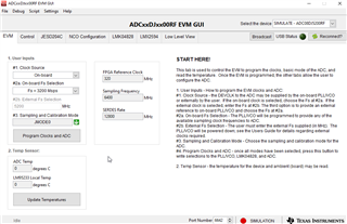
    I did just test out the EVM in the GUI as suggested by configuring with Fs = 3200 Msps setting, using a 320 MHz ref clock. What should the signal generator (external reference) be providing for any GUI config?


    Even in this configuration set up, however, the serializer PLL is still not reading back locked status.


    The reason for the more complex clocking scheme is because of our custom DSP architecture needs.

  • Eric,

    I want to shed light and perhaps open a discussion on what I am observing by scoping LMX output:  

    When using a valid LMX TICS config (file attached), we are probing a stable clock on RFoutA at 700 MHz (N divider = 28, Fosc = 400 MHz).

    When using this valid TICS config to output 800 MHz on RFoutA, the probed clock signal is visibly smaller and less stable. On the scope it appears to inherit some sort of periodic amplitude DC offset (not sure what this is called nor the cause/effect).

    With this same config, by scoping as I increase the N divider value up to the maximum allowable (N = 38, giving RFoutA = 950MHz), I see the amplitude decrease significantly. 

    Once Fvco reaches the 11500 MHz threshold, I modify Channel Divider to hold a value of 8 which reduces the Fvco to a valid range and allows me to continue bumping up the value of N. At the point RFoutA becomes 1050 MHz (N divider = 42) the output signal quality and amplitude diminishes quite noticeably to the extent that it appears that we are scoping noise. 

    Unless we are missing something or this is an unusual characteristic indicating a damaged device, I am unsure how it is possible to modify this output so as to generate a reliable clock signal to be used as input into the ADC.

    Please let me know your thoughts here--I believe it is essential to address this for the serializer PLL to ever possibly lock at a desired clock frequency of 3200 MHz and above.

    Your input is greatly appreciated!

    LMX-400in-NdividerSweep-Scope.tcs

  • Hello Michael,

    The serdes pll of the adc should be able to lock to any valid frequency of the given ADC JMODE it is in, so the the problem could potentially be that there is not enough power at the ADCs clock input or the frequency being input is an invalid frequency.

    I have verified on the EVM that this mode works when I program it with the ADC GUI pll locks and I am able to capture data. However I have noticed that when I try and program the ADC and lmx through configuration files I cannot get the link to work can we try and program everything through the ADC GUI and see if that changes anything.

    To get the link to work I am using the settings...

    external reference, on board selection=3200 and JMODE0 with a reference signal to the Board of 320 MHz at 9dBM. Can you please try and replicate this setup and see if you have any luck.

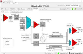
    Also the config file you provided for the lmx is not what you are using to supply a clock to the ADC correct? If this is the file I cannot see how this would work there is no value of the channel divider that can get you 3200 MHz. I have gone through and calculated the values to use for the lmx can you please try setting these in the ADC GUI and then checking the serdes pll lock status. This is calculated assuming a 400 MHz reference at the ADC 

    Can you also share the output power setting on the LMX you are using and match them to the default programmed to the gui.

    Also can you share the hardware modifications you made to the board I would like to double check these.

    Thanks,

    Eric

  • Eric,


    Thank you for your feedback, it is very helpful. When configuring the board using the GUI settings you suggested, the Serializer PLL is not locked.


    Sorry for the confusion; the LMX configuration I sent was to spotlight the LMX output clock signal. I was testing lower clock frequencies to observe on a scope what exactly is being provided to the ADC. And it appears that our LMX output diminishes in both amplitude and signal quality to the extent that any output clock signal beyond 1.2 GHz appears nearly indistinguishable from noise.


    The output power setting on the LMX is 63 on RFoutA (R 0x2C3F00)


    The hardware modifications are exactly as listed in section 7.2.3 of the EVM User Guide: we populated R171 and R174 with a 0ohm 0201 resistor and populated C52 and C306 with the removed capacitors C60 and C61