This thread has been locked.

If you have a related question, please click the "Ask a related question" button in the top right corner. The newly created question will be automatically linked to this question.

DAC38RF82EVM: Signal loss at the DAC output when increasing the number of serdes lane

Part Number: DAC38RF82EVM
Other Parts Discussed in Thread: DAC38RF82

Hello,

I am evaluating DAC38RF82 with the evaluation board and the pattern generator.

A 100 MHz / +6dBm signal is fed to the input of the LMK (J4 connector).

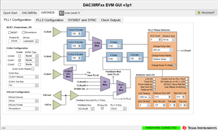
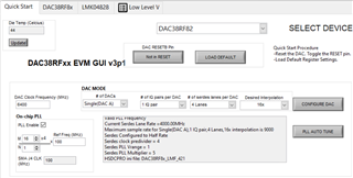
With the following configuration (only one DAC), all is right, a correct spectrum is present at the output of the DAC.

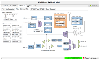
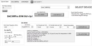
When the configuration is changed to 8 lanes (instead of 4 lanes), the Serdes Lane Rate is twice lower, there is no other configuration change than the HSDCPRO file (suffix 821 instead of 421) : 

On the HSDCPRO GUI, when loading the right ini file (suffix : 821), the following pop-up message appears:

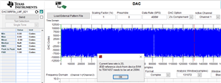
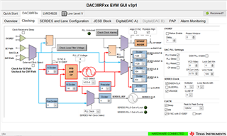
And after resetting DAC JESD Core (DAC GUI), it is not possible to have a spectrum at the DAC output (no signal at all).

I suppose that this is due to the JESD reference clock (to TSW14J57) which has to be set to 200 MHz (instead of 100 MHz).

What is wrong with this configuration ?

  • Hi Alain,

    I suspect the issue is with the LMK divider for the FPGA. Can you show the PLL1 and PLL2 configuration tabs and also the output dividers tab?

    Thanks, Chase

  • Hi CHase,

    Here are the requested information for this setting.

    LMK PLL1 configuration:

    LMK PLL2 configuration:

    LMK Clock Outputs:

    DAC Clocking tab:

    Alain

  • Hi Alain,

    The issue does come down the the FPGA reference not being correct, but the GUI is doing a few more things incorrectly here. For 6400MSPS, 16x interpolation, in 421 the FPGA wants a 100MHz reference, however when changing to 821, the FPGA wants a 200MHz reference.

    In the 821 mode, the GUI is for some reason setting the LMK output as below, with FPGA being the J4 reference /2 and the DAC matching the J4 reference. This is incorrect. 

    If you provide a 200MHz reference into J4, set the FPGA DCLK divider as 1 and the DCLK source as Bypass, the FPGA will correctly receive the J4 (200MHz) / 1 = 200MHz.

    For the DAC, you have a few options:

    1. You can change the M divider from 16 to 8 and double the reference from 100MHz to 200MHz. In this case, the DAC and FPGA clock will match and no further action is needed. The DAC VCO frequency would then be 8/1*4*200MHz = 6400MHz.
    2. You can set the DAC DCLK divider as 2 and the DCLK source as Divider, this will set the DAC reference as J4 (200MHz) / 2 = 100MHz. The DAC VCO frequency would then be 16/1*4*100MHz = 6400MHz.

     Thanks, Chase

  • Hello Chase,


    If I well understood, when you wrote “the FPGA wants a 200MHz reference”, this is due to the evaluation board and pattern generator architecture, isn’t it ?

    Do you confirm that there is no limitation from the DAC chip ?

    It mean that, in our own design using this DAC, it will be possible to use 8 lanes with 6400MSPS, 16x interpolation and 100 MHz frequency reference sent to the DAC, correct ?


    Alain

  • Hi Alain,

    The DAC is fine as is and can use the 100MHz reference, yes. The issue is the serdes transceiver on the fpga demo board is requiring a 200MHz reference, I am guessing it has run out of divider adjustment for the PFD into the serdes transceiver PLL. As on the other post, I'd start looking at FPGA JESD IP cores to see what is required by the JESD core for this DAC operating mode. I can't guarantee the FPGA clocks, however I can guarantee the DAC will operate without issues when using the PLL settings with the 100MHz reference: 16/1*4*100MHz = 6400MHz.

    Thanks, Chase