This thread has been locked.

If you have a related question, please click the "Ask a related question" button in the top right corner. The newly created question will be automatically linked to this question.

ADS122C04: Differential Measurement Input matching and ESD Diode Activation

Part Number: ADS122C04

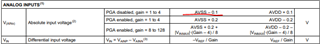
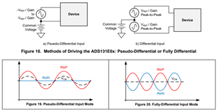
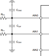
We are using Ain0 and Ain1 to measure a pseudo-differential  ±2.0V signal. We have ±2.5V for AVDD and AVSS and are using AVDD and AVSS as references. The current termination of the signal before the ADC inputs is a configuration of 10nF for Cdiff and 1nF for Ccm. We are not using the PGA and have set the register to bypass it.

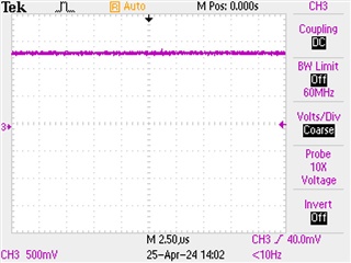
The problem is that it appears that the internal ESD diodes are activating for signals larger than 60-70mV, driving the readings to 0V.

We have tried varying Cdiff and Ccm, adding inductors before Ain, adding resistors before Ain, and changing the common mode voltage from -2.5V to 0V.

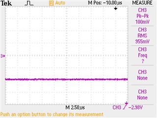
We have had some measured progress with the above, measuring voltages up to 700mV before the diodes would activate. Unfortunately we have not yet been able to perform full-scale measurements.

Any assistance or reference documents on how to terminate a differential input would be greatly appreciated.

  • Hi Augustine,

    AVDD and AVSS as references

    By this do you mean that you connect VREPP to AVDD and VREFN to AVSS?

    Can you try connecting RFEFN to GND rather than AVSS(-2.5V)?

    You could also just use the internal voltage reference which would allow you to measure from -2.048V to +2.048V which should be sufficient for a +/-2V signal. 

    changing the common mode voltage from -2.5V to 0V.

    By this do you mean that AIN1 (AINN) is tied to AVSS(-2.5V)? 

    If this is the case and then you are applying a +/-2V signal to AIN0 (AINP) the signal would swing between -0.5V to -4.5V which is outside of the range you can measure. 

    Can you provide a schematic and show what signals exactly are being applied to which pins? That would help a lot in clarifying what you are doing and to determine what the problem is.

    Best Regards,

    Angel

  • Hello Angel, thank you for your reply.

    VREFP & VREFN are floating, the ADC122C04 can use AVDD and AVSS as the reference (muxing them internally). I have also used the internal 2.048V reference but experienced the same issues.

    Below is a schematic that shows that I am using AVSS as the common-mode voltage. Your explanation does make sense and I was thinking along these lines earlier and modded a board so that AIN0 and AIN1 were coupled to ground instead. Unfortunately, I was not able to read full-scale and the diodes would shunt current to AVSS and AVDD.

    The capacitor values have been changed multiple times and I have pulled traces to put resistors before the analog inputs. This did not work.

    The input signal is buffered, filtered and has 2.4V Zeners for over-voltage protection.

    AIN2 and AIN3 are used for an RMS-to-DC converter with an output from 0V to 1V. This works as expected and I have no issues with it.

    I greatly appreciate your time,
    Augustine

  • Hi Augustine,

    I don't see how your schematic shows you are using AVSS as a common-mode voltage. What you are showing is that you are connecting the filter capacitors to AVSS. 

    Are you connecting any input pin directly to AVSS?

    Common-mode volage is defined as Vcm = (Vp + Vn) / 2 you can think of it as the average of the voltages applied to the input pins. 

    If you were to tie AINN to GND or AVSS and a sine wave to AINP, the common mode voltage Vcm would be a sinusoidal as well that's in between the voltages applied to AINP and AINN. This would be a pseudo-differential signal. Below is an example: 

    Maybe there is a misunderstanding when you mention using AVSS as the common-mode voltage. 

    If Vcm = -2.5V (AVSS), applying a Vdiff of +/-2V would mean you are trying to measure a signal that between -0.5V and -4.5V, this would be outside the +2.5V to -2.5V of your supplies. 

    The purpose of the capacitors should be to serve as anti-aliasing filters, something like this: 

    The differential capacitor should be sized 10 times the common-mode capacitor. This sets the differential mode cutoff frequency about 20 times lower than the common-mode cutoff frequency. This prevents common-mode noise from being converted into differential noise due to component tolerances.

    Can you specify exactly what you are applying to the AIN0 and AIN1 input pins?

    Best Regards,

    Angel

  • Hello Angel, thank you again for your reply.

    The input to AIN0 is a ±2V DC signal referenced to AIN1. Having a potential difference of more than 700mV DC between AIN0 and AIN1 causes the ADS1220C04 to activate the protection diodes.

    I apologize, referring to the input signal as pseudo-differential was a mistake. The signal is probably better described as a buffered uni-polar signal from AIN0 to AIN1.

    Today we have modified the input so that the filter caps are now going to ground (as you have shown in your second image) and we changed their values such that Cdiff is 10nF, and Ccm1 and Ccm2 are 1nF.

    I cannot really share any more of the schematic publicly, but I can provide a simplified schematic if you would like. Or if there is a way confidentially share the schematic, that would be fine as well.

    Thank you for your time,
    Augustine

  • Hi Augustine,

    causes the ADS1220C04 to activate the protection diodes

    What leads to this conclusion and how can you verify? It seems unlikely that this is the problem.

    The signal is probably better described as a buffered uni-polar signal from AIN0 to AIN1.

    Since you mentioned that the signal is buffered, have you verified for oscillations at the output of the buffer due to op amp instability? This may be a problem since you would be driving a capacitive load at the output of the buffer due to the ADC input filter capacitors. Can you probe the analog inputs/buffer output with an oscilloscope and share what you see? This would also help clarify what your actual input signal looks like.

    Best Regards,

    Angel 

  • Hello Angel, thank you for replying and I am sorry for my delay in responding.


    We are assuming that the ESD diodes are are activating because the ADC reports 0x000000 and either AVDD or AVSS has current shunted to it, raising the absolute potential with reference to ground.

    Here is an approximate +1V signal from AIN0 to AIN1:

    The output codes from the ADC for the signal above are what we would expect, 0x2177D7. Which would roughly be 1.282V.

    Here is an approximate -1V signal from AIN0 to AIN1:

    The ADC reports 0x000000 for the signal above and AVSS goes from -2.49V to -4.53V.

    I find this very confusing and the only mechanism I have been able to consider is the ESD diodes are activating.

    Thank you again, and I appreciate your time.
    Augustine

  • Hi Augustine Savoca,

    Angel is out of the office today, we will respond to you next week. Thanks for your patience

    -Bryan

  • Hi Augustine,

    Thank you for providing these captures. 

    You are showing the differential voltage between the two input pins in the scope captures (AIN0-AIN1), but the voltages may be floating if they aren't being referenced to anything. 

    Would you be able to show the voltage at the AIN0 pin with respect to GND, and the Voltage at the AIN1 pin with respect to GND separately? 

    The absolute voltages at each of the input pins should be in-between -2.5V and +2.5V (your analog supplies).

    For example, if the absolute voltage with respect to ground at AIN1 is -2.5V, and the absolute voltage at AIN0 is -1.5V, Vdiff (AIN0-AIN1) would be = +1V, and your output code (~0x2177D7) and scope capture from AIN0(+) to AIN1(-) would show this. This would be valid since the absolute voltages at both input pins with respect to GND are within your supplies (-2.5V to +2.5V).

    However, if the absolute voltage at AIN1 is -2.5V, having a Vdiff of -1V would mean that the absolute voltage at AIN0 would be at -3.5V. [ Vdiff = AIN0 - AIN1 = (-3.5V) - (-2.5V) = -1V ]. Your scope measurement between AIN0 and AIN1 would show -1V, but the actual absolute voltages at the input pins would be outside of the recommended operating range (-2.5V to +2.5V) and this could damage the device or cause unknown behavior. 

    Not completely sure if that is what is happening here, but it seems like that could be what the problem is. 

    Best Regards,

    Angel