This thread has been locked.

If you have a related question, please click the "Ask a related question" button in the top right corner. The newly created question will be automatically linked to this question.

ADS1262: RDATA returns highest possible number no matter what

Part Number: ADS1262

I'm using the ADS1262 with a custom pcb. I can read and write config registers perfectly fine but when I do a RDATA command I always get back 01111111 11111111 11111111 11111111 as the response no matter what.

Is there a common cause for this? All settings are set to default aside from turning off the checksum and status bytes for simplicity. I followed the flow chart in the datasheet as best I could but I get this result no matter what. Doubling the size of the transmission data buffer repeats this output. Is it some king of shifting error or am I missing a setting? Any insight is much appreciated.

  • Hi Alex Moran,

    Typically a full-scale output code is a result of a missing reference voltage or using a large gain for a large input signal.

    The ADC output code is ~VIN/VREF, so if VREF = 0 the output code will be maxed out. Or, if VIN>VREF, then the output will always be max code.

    Let me know if either of these are the case in your system

    -Bryan

  • I set the config registers to use the internal voltage reference and the gain is currently set to 4.  Ive also tried with the gain set to 1 with the same results. 

  • Hi Alex Moran,

    What is the input signal you are applying? And how is that signal referenced to the ADC ground?

    If you measure REFOUT, is it 2.5V?

    If yes, can you apply REFOUT to two of the ADC input channels e.g. AIN0 and AIN1, so they are shorted together, then set the gain to 1 and measure a few hundred samples at a reasonable data rate e.g. 500 samples at 400 SPS, and let me know what you get?

    Finally, how are you reading back data? Are you using the DRDY pin to trigger reading data?

    -Bryan

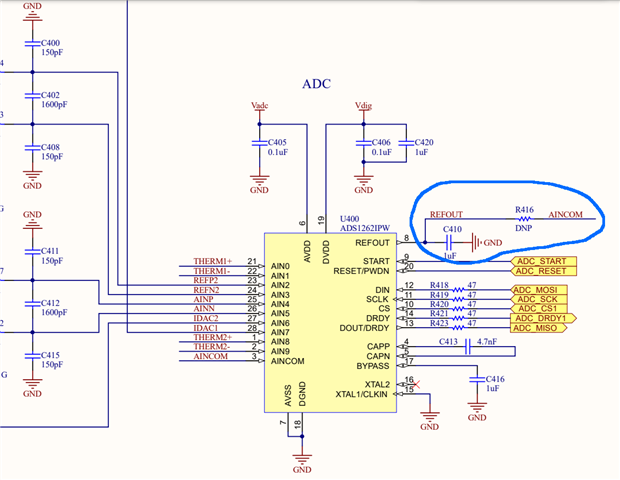
  • The input signal is just a type K thermocouple. I tried measuring REFOUT and I'm getting 0V. That definitely seems to be the source of the problem because VIN is always greater than VREF if its 0. The problem now is why is that giving me 0V even when I'm using the internal reference. I noticed in our schematic that it looks like REFOUT is tied to AINCOM is that normal? Is there a reason why it would be that way or is that wrong? Picture of the schematic for reference.

  • Hi Alex Moran,

    You can connect REFOUT to AINCOM, that should not be an issue. This will allow you to take pseudo differential measurements if you have single-ended input signals 

    You said you can read and write registers perfectly fine, can you confirm that the registers are all in the default configuration after power up?

    If you can write registers, can you change the REFMUX register to use either the external ref inputs or the supply, then see if the ADC behavior changes? Make sure to read back any registers you write to confirm that the WREG took effect

    Can you also confirm that if you take the START pin high after power up do you see the DRDY pin pulsing at a frequency of approximately 1/default data rate, which in this case is 20 SPS (or a pulse every 50ms or so)?

    You should also start by measuring a known signal from a precision source instead of a TC. For example, a AA battery is 1.5V. This way you know what to expect as the ADC output code.

    -Bryan