


Dear TI,
I have the following report of an issue with the ADS8681 part. We would like to get in contact with a FAE about this, or receive hints to potential causes from people who have experience with this part. Thanks!
Executive Summary
This report details the intermittent erroneous readings observed in several ADCs across different boards. The issue has been analyzed using advanced diagnostic techniques, including FPGA-based signal sampling at 200MHz and real-time signal monitoring using a logic analyzer. Crucially, these faulty ADC samples lead to dramatic malfunctions in the controller behavior, potentially compromising system stability and performance. This underscores the urgency of addressing these anomalies to prevent operational failures.
Introduction
The ADCs have exhibited sporadic faults, characterized by incorrect single sample readings. Initial hypotheses focused on SPI communication errors, both in Dual and Single SPI modes. This report explores beyond preliminary assessments, incorporating hardware-level signal integrity and sampling strategies.
Problem Statement
Erroneous ADC readings persist despite variations in SPI communication modes and clock speeds, indicating potential internal ADC malfunctions or external signal integrity issues.
Methods and Materials
FPGA Sampling: Utilized an FPGA to sample the ADC input signals at a high frequency of 200MHz, aiming to capture detailed signal behaviors.
Logic Analyzer: Redirected sampled signals to a logic analyzer for extensive real-time analysis, facilitating a deep dive into the timing and integrity of the ADC's data output.
SPI Mode Variations: Tested both Dual and Single SPI modes under different clock settings (specifically at 12.5MHz) to assess the impact on ADC performance.
Signal Integrity Analysis: Conducted thorough inspections of signal paths, voltage levels, and grounding to identify any contributing factors to signal degradation.
Observations and Results
No Influence from Probing: Confirmed that the monitoring setup, including the connection of probes and redirection of signals, does not alter or interfere with ADC operations.
Persistent Errors Across Settings: The occurrence of errors remains consistent across different operational modes and settings, reinforcing the notion that issues may stem from within the ADC or its immediate signal environment.
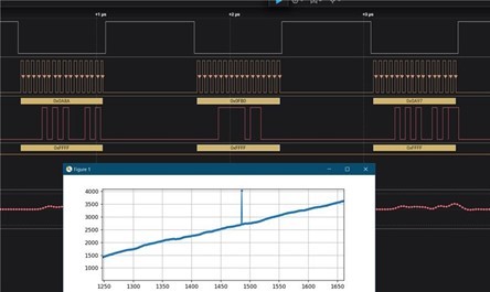
Figure 1: Wrong sample at 25 MHz SPI Clock
The figure below illustrates a faulty sample captured while the SPI clock was set to 12.5MHz. It displays the input data from a logic analyzer, which records at a rate of 500 million samples per second. The image shows the analog signal of the MISO-0 line, which exhibits activity. In contrast, the MISO-1 line remains consistently high, showing no variation or activity. This visual representation aids in understanding the dynamics of the signal and identifying the timing of the error.
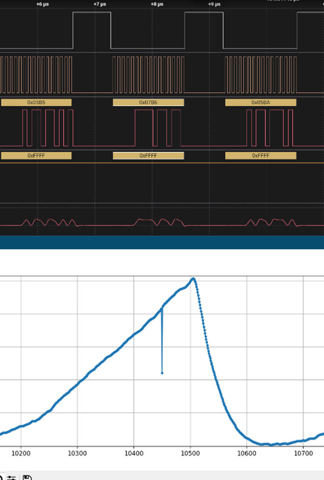
Figure 2: Wrong sample at 12.5 MHz SPI Clock
Discussion
The analysis suggests that the ADC errors are less likely due to SPI communication faults and more likely linked to internal ADC errors or external signal disturbances. Given the high-resolution sampling and real-time analysis capabilities, the findings strongly point towards intrinsic ADC susceptibilities to certain conditions, possibly overlooked during the ADC design or manufacturing process.
Conclusion
The investigation documented in this report confirms intermittent and erroneous readings from the ADS8681, which critically impact controller operations and overall system reliability. These malfunctions are not only disruptive but could lead to significant operational failures if not addressed promptly.

