Because of the Thanksgiving holiday in the U.S., TI E2E™ design support forum responses may be delayed from November 25 through December 2. Thank you for your patience.

This thread has been locked.

If you have a related question, please click the "Ask a related question" button in the top right corner. The newly created question will be automatically linked to this question.

DAC81416: DACPWDWN not holding its value

Part Number: DAC81416

I can write and read from DEVID, and write to SPICONFIG and verify the value by reading it back. I can also enable the internal voltage reference and verify 2.5V at the output. So the SPI communication is definitively OK.

But when I write to DACPWDWN, I allways get 0xFFFF when reading back. Writing to the DAC ouput values allways gives 0 as readback, but this is probably because the DAC registers are write only (according to an old post). There is no output on the output pins. This is tested with range 0-5V.

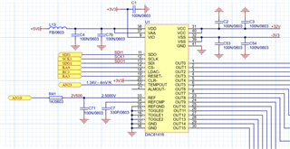
The CLR and RST pints are both 3.3V.  The CLR is connected directly to 3.3V. All supply voltages are ok.

The old post indicates a similar problem, but there is no solution to the problem.

  • I have found something disturbing. The Temperatur alarm bit is set (Actually the STATUS is 0x0009). And the tempertature output voltage is +5V!!!

    Could the temperature sensor be damaged, and the chip believes it is in over-temperature? 

  • Further testing gives correct temperature output of 1.25V (22.5C) which is correct. But this happens only after the internal voltage reference is turned on. Before that, the temperature output is +5V. This is an unloaded output so possibly a small load would pull the output down to 0V. When tested, a 4k7 load makes the output drop to ca 4.1V,

  • Hi Jan, 

    Sanjay will review and provide a response soon. 

    Are you using the EVM or a custom board? If it is an EVM, can you share your jumper settings and what supplies you have connected? If it's a custom board, can you please share a schematic with all of the supply voltages shown?

    Best,

    Katlynne Jones

  • Hi Jan,

    Please provide details as mentioned by Katlynne and also the DUT supply values along with SPI command sequences used for device wake up.

    Regards,

    Sanjay

  • It is not the evaluation board, but my own layout. The voltage called +33V has now een reduced to +12V. The connection to the AN23 input on the CPU has been cut because the voltage goes to +5V at reset. It goes to 1.25V ater initialization. The reference voltage output at 2.500V is ok when enabled.

    The code is as follows. The constants are as given in the datasheet, and the code should be self explanatory. The code can correctly read and write to the registers - all the tests are ok - no halt() is called.  The readback of the status register gives a value of 9. Bit 0 and 3 are set. Bit 0 is TEMP-ALM, but bit 3 is not described in the datasheet. Does it meen anything?

    DAC16_RESET_LOW;
    time_spin_us(1);
    DAC16_RESET_HIGH;
    time_spin_ms(1);
    // Verify ID
    if ((dac16_read(DEVICEID) >> 2) != 0x29C) halt(DAC_ERROR);
    // Verify default SPICONFIG contents
    if (dac16_read(SPICONFIG) != 0x0AA4) halt(DAC_ERROR);
    // Turn off power down and enable SDO output
    dac16_write(SPICONFIG, 0x0A84);
    if (dac16_read(SPICONFIG) != 0x0A84) halt(DAC_ERROR);
    // Enable internal voltage reference
    dac16_write(GENCONFIG, 0x3F00);
    // Try resetting overtemp alarm
    dac16_write(TRIGGER, 0x0100);
    // Enable all channels
    dac16_write(DACPWDWN, 0x0000);
    reg = dac16_read(DACPWDWN); // Returns 0xFFFF, not 0x0000 as it should !!!!
    reg = dac16_read(STATUS);  // Returns 0x0009
    // Set All channel ranges to 0-5V
    dac16_write(DACRANGE0, 0x1111);
    dac16_write(DACRANGE1, 0x1111);
    dac16_write(DACRANGE2, 0x1111);
    dac16_write(DACRANGE3, 0x1111);
    // Set all outputs to 2.5V
    for (i = 0; i < 16; i++) dac16_write(DAC + i, 0x8000);
    // Toggle LDAC just in case it is needed
    DAC16_LDAC_LOW;
    time_spin_us(1);
    DAC16_LDAC_HIGH;

  • Hi Jan,

    Could you also please share the schematic design after all DAC0 - DAC15 channels ?

    Thanks,

    Sanjay

  • The outputs are currently not connected to anything. The plan is to connect them to a pin in a "Bed of nails" through a 100ohm resistor.

  • Hi Jan,

    Can we connect for a short meeting and do a live debug session ?
    I have sent the details via mail.

    Regards,

    Sanjay