This thread has been locked.

If you have a related question, please click the "Ask a related question" button in the top right corner. The newly created question will be automatically linked to this question.

AFE5816: Problems in AFE output test pattern data

Part Number: AFE5816

Hello, everyone

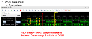
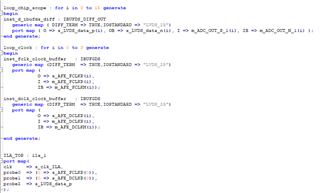
I am trying to verify the output from the AFE using a test pattern. I want to check the output data through ILA, and the clocks are as follows: ILA clock = 280MHz AFE input clock = 10MHz It is set to 14bit 1X serialization.

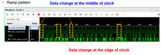
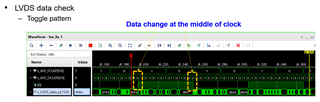
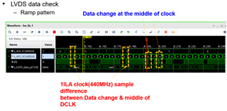
In the toggle pattern, as in the datasheet, we can see that the data changes at the center of DCLK. However, in the ramp and sync, some of the data was observed to change at the edge of DCLK. What could be the potential problem and solution?

1) SYNC pattern (works wrong)

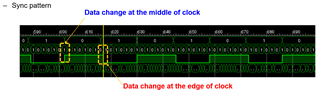
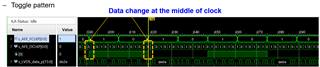
2) Toggle pattern (works well)

3) RAMP pattern (works wrong)

  • Additionally, s_AFE_DCLKP is my dclk and s_AFE_FCLKP is my fclk and (0) is output data from AFE. 

    And these are my register setting sequences

    1) Hardware reset signal for 100ns

    2)

    Register 1 , Value 14

    Register 41 , Value 8000

    Register 42 , Value 8000

    Register 41 , Value 0000

    Register 42 , Value 0000

    Register 3 , Value 2010

    Register 4 , Value 0001

    Thank you.

  • Hi,

    Did you check the ADC supply is clean ?

    Also can you check ADC_CLK is not corrupted ?

  • Hi my ADC supply is clean, and this is my ADC_CLK.

    Is there anything wrong??

    In datasheet, required ADC_CLK is 

    1) Common mode voltage = 0.7V

    2) Differnetial Swing = 0.35V

    And this is my supply ADC_CLK

    1) Common mode voltage = 750mV

    2) Differential Swing = 0.4V


    I don't solve the problem mentioned above. Is there any recommendation to solve this problem??

  • Hi,

    I believe this is FPGA related issue. Device should not behave like this .

    Device DCLK will be at 70MHz and you are sampling this in 280MHz ILA clock . Because of this resolution captured data might not be looking correct. 

    1) Can you check this data at device output on scope to verify the same signature ? This is to verify the device output is coming as expected .

    2) Can you change the ILA clock to 560MHz and check this again ?

  • Hi, I tried again with the changes you told me

    For ILA  resolution,

    FCLK = 7.85714MHz

    DCLK = 55MHz( 14bit 1X serialization.)

    ILA = 440MHz

    Still, there are differences between test patterns.

    With better ILA resolution, still there are timing error in ramp pattern & sync pattern.

    This is my VHDL code about LVDS code & ILA.

    Is there any problems to cause theses difference??

  • With the updated ILA frequency now you are able to see that data is not changing in the clock edge . 

    You are observing some difference in data change with respect to clock . This can be due to quantization of sampling clock (ILA clock). If data is changing when the ILA clock is sampling it can have that once ILA clock uncertainty and which is what you are seeing.  

  • Thank you, 

    The data does not change at the edge of the clock.

    However, the timing between test patterns is different. What could be the reason for this?

    Even if the register setting or the clock is not wrong, is it possible for the timing to not match exactly?

  • There can be slight timing mismatch. Also your FPGA delays for each path also comes into picture. Once you capture the LVDS Data you should not face any issue .