This thread has been locked.

If you have a related question, please click the "Ask a related question" button in the top right corner. The newly created question will be automatically linked to this question.

ADS54J69: ADC is not responding on SDout line

Part Number: ADS54J69
Other Parts Discussed in Thread: ADS54J60

Hello,

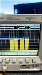
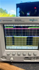
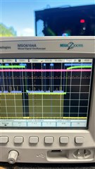
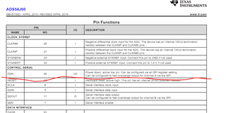
We are trying to configure our ADS54J69 on our custom FMC board. With an oscilloscope we see data coming from the FPGA to the ADC on the SDIN line, we see the correct SPI clock on SCLK, and our reset line is behaving correctly.

However, we are not seeing any data on SDout which is telling us the ADC is unresponsive.

We are writing these values to the registers to set the ADC to LMFS-4211:

// FMC231 ADS54J60 settings
// LMFS = 4211 no Decimation mode. this mode is only for ADS54J60. JESD204 lane 0 = DA1; lane 1 = DA2
static spi_bus_t ads54j60_4211_init_regs[] =
{
// register writes reset
{{0x00, 0x00}, 0x81}, // Reset registers in the ADC and master pages of the analog bank.

{{0x40, 0x01}, 0x00}, // Clear any unwanted content from the unused pages of the JESD bank.
{{0x40, 0x02}, 0x00}, // Clear any unwanted content from the unused pages of the JESD bank.

{{0x40, 0x03}, 0x00}, // Select the main digital page of the JESD bank.
{{0x40, 0x04}, 0x68}, // Select the main digital page of the JESD bank.

{{0x60, 0xF7}, 0x01}, // Use the DIG RESET register bit to reset all pages in the JESD bank.

{{0x60, 0x00}, 0x01}, // Set PULSE RESET register bit for channel A
{{0x60, 0x00}, 0x00}, // Cler PULSE RESET register bit for channel A

// performance mode
{{0x00, 0x11}, 0x80}, // Select the master page of the analog bank.
{{0x00, 0x59}, 0x20}, // Set the ALWAYS WRITE 1 bit.

// Select the JESD digital page
{{0x40, 0x04}, 0x69}, // Select the JESD digital page
{{0x40, 0x03}, 0x00}, // Select the JESD digital page

// Select the CTRL K bit
{{0x60, 0x00}, 0x80}, // Set the CTRL K bit for both channels by programming K according to the SYSREF signal later on in the sequence.

// enable scrambling
{{0x60, 0x05}, 0x80},

// K=32
{{0x60, 0x06}, 0x1F}, // Frames per multifame

// Select the digital to 40x mode
{{0x60, 0x01}, 0x04}, // Four lanes are active, no decimation (filter bypass), Use the SYNC pin for sync requests, Normal operation
//Or test mode
// {{0x60}, {0x01}}, {0x84}, // Four lanes are active, no decimation (filter bypass), Use the SYNC REG register bit for sync requests, ADC output data are replaced with K28.5 characters.

// Select the JESD analog page
{{0x40, 0x04}, 0x6A},
{{0x40, 0x03}, 0x00},

// Set the SERDES PLL to 40x mode
{{0x60, 0x16}, 0x02},

// PLL reset
{{0x60, 0x17}, 0x40}, // PLL reset set
{{0x60, 0x17}, 0x00}, // PLL reset clear

/* // transmitter amplitude
{{0x60, 0x1B}, 0x60}, //[7:5] JESD swing. 0=860mV 1=810 2=770 3=745 4=960 5=930 6=905 7=880 [3] FOVR CHA en

// de-emphasis
{{0x60, 0x12}, 0x04}, //[7:2] de-emphasis 0=0dB; 1=-1 3=-2 7=-4.1 F=-6.2; 1F=-8.2 3F=-11.5
{{0x60, 0x13}, 0x04},
{{0x60, 0x14}, 0x04},
{{0x60, 0x15}, 0x04},
*/
// Select the main digital page
{{0x40, 0x04}, 0x68},
{{0x40, 0x03}, 0x00},

// Pulse the PULSE RESET regiter bit
{{0x60, 0x00}, 0x01}, // Pulse the PULSE RESET register bit. All settings programmed in the main digital page take effect only after this bit is pulsed.
{{0x60, 0x00}, 0x00}, // Pulse the PULSE RESET register bit. All settings programmed in the main digital page take effect only after this bit is pulsed.

{{0x00, 0x00}, 0x00} // The last
};

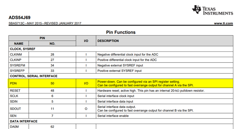
Our PDN pin is tied high in our design and our firmware and SPI settings above do not address this pin and we are not planning to use the power down mode.

Can the settings above be checked and is there anything that needs to be done with the PDN pin?

Thank you,

Ryan

  • Ryan,

    I'm not familiar with this device but quickly looked at this. Have you tried writing to set the OVERRIDE PDN PIN field high and then toggle the GLOBAL PDN field high? You could then look at the supply current to see if it drops when the GLOBAL PDN field is asserted or not. This would tell you if the SPI is getting through to the device while removing the PDN pin entirely.

    Chase

  • Hey Chase thanks for your response!

    Unfortunately toggling the PDN pin did not work. We have set this pin low and have set this pin high and we see the same result either way. 

    To clarify we are only resetting the ADC after it has received the clocks and power. We are at a bit of a loss of what is going wrong.

    Can the settings above be verified for LMFS=4211?

    Thanks,

    Ryan

  • Also for more information, our current sequence is the following:

    1) Power up
    2) RESET for Clock, DAC, ADCs. PDN for ADC at 1 (optionally to 0)
    3) Embedded Linux starts
    4) Clock is programmed (we now have clocks)
    5) RESET ADC again
    6) try to program register and readback.

  • Hello we are also using a DAC, DAC39J8, and this device is also failing to respond over SPI. I am including oscillograms of the SPI lines as they go into the ADC (specifically a read from the 0x04 register). The yellow trace is the SPI CLK shared between the two ADCs, the green trace is the SEN signal (we have two ADS54J60 on this board, the oscillogram is just looking at the SEN for one of the ADCs which is why activity is present on SDin (SPI in) which is shared between the two ADCs), the blue trace is SDin (SPI in), and the pink trace is the SDout (SPI out line):

  • Hello,

    We are stuck on this! Can we please get some ideas/assistance as of what we can try?

  • Hi Ryan,

    Do you see a change in supply current when programming either the ADC or DAC?  This will tell us if the device is "seeing" the SPI transaction.

    Regards,

    Geoff

  • Hello Geoff,

    We do see the supply current increase during SPI writes. For the DAC we figured out part of the problem, the data sheet says that the SDout pin is push-pull, but in fact this pin is open-drain, so we applied a 1k ohm pull-up resistor and now can successfully read registers from the DAC.

    We tried a similar pullup on the SDout lines for the ADC but are still not seeing activity on this line. We do see current consumption increase when we write to the ADC though. Is there some register on these ADCs that must be written to enable a driver for SDout that is not mentioned in the datasheet?

    Thanks,

    Ryan

  • Hello Geoff,

    We eventually figured out that if the pull-up resistor to 1.8V is removed from the PDN line, that the ADC device operates correctly. From the datasheet we had the impression that the PDN pin is active low:


    However, we learned that when the PDN pin is high, that the ADC is in a powered down state. Is this difference from the documentation for this pin correct? It seems our whole system is working successfully now with this change. 

    Thanks,

    Ryan

  • Ryan,

    That would make sense. The document online for ADS54J69 shows active high powerdown. What document are you looking at in the previous post snippet? Below is from the ADS54J69 datasheet. 

    Thanks, Chase

  • Hey Chase,

    This board has the ADS54J60 installed. However, the datasheet still has PDN as being active low in it.

  • Thanks Ryan, I'll notify our team of the fix.