This thread has been locked.

If you have a related question, please click the "Ask a related question" button in the top right corner. The newly created question will be automatically linked to this question.

ADS52J90: Analog input termination and coupling

Part Number: ADS52J90

I can't find this one being asked previously. I am interfacing the ADS52J90 inputs to 100Ω differential (Zdiff) analog outputs from another device. The datasheet figure 89 is as follows but I don't understand why it has both 100Ω and 50Ω termination. I believe it is both terminating a 50Ω pair with VCM, and showing 100Ω termination as well (not necessary to do both)? If both are intended to be present then this would present a impedance mismatch.
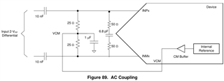
Figure 90 of the datasheet (DC coupling) shows just the 100Ω termination.

I've derived this based on the EVM schematic including 50Ω termination fitted as it includes ADT1-6T (1:1 50Ω) baluns:
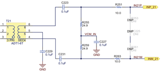
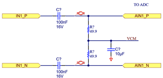
I have used basically the EVM circuit (without the 50Ω resistors and 6.8pF cap) but changed the 24.9Ω resistors to 49.9Ω for my 100Ω Zdiff system, as shown below (representative of my system). Is this not the right way to terminate the diff pair and inject VCM?
  • Hi,

    The first 50 ohm and 6.8pf is not for termination . This is used to absorb sampling glitch from the device .  The corner frequency of this is designed for that .  This is explained in the datasheet also.

    Are you using ac coupling or dc coupling ?

  • Hello Sachin. Thanks for your response. The datasheet, from my reading of it, doesn't say anything about sampling glitches or the 2 x 50R and 6.8pF capacitors. I read this part to be talking about the 2 x 25R and 1uF VCM injection circuit because it's immediately after the sentence talking about VCM injection:

    The resistor and capacitor values used for coupling determines the high-pass filter corner of the input circuit; thus, these values are chosen with the frequency of interest in mind.

    But it could, I suppose, be talking about all the R's and C's on the input circuits.

    Are you able to guide me on the glitch sampling absorption circuit then? It looks to be a low-pass filter with a -3 dB point at around 460 MHz. Is this necessary for SNR/SINAD purposes, and at what frequencies? A response ASAP would be appreciated as I'm late in the design phase. Thanks!

  • Hi Corey,

    Because of ADC sampling circuit there will be high frequency glitch at the input . To absorb that glitch 50 ohm and 6.8pf is placed . This will form HPF to attenuate those glitches .These can be modified according to your needs . This corner should lie outside of your signal bandwidth . If you dont have this option this glitch can reflect back and effect next sample which effects SNR.