Other Parts Discussed in Thread: LMK04828, LMX2594, LMK61E2, LMK00304
I have some questions about ADCxxDJxx00RF Evaluation Module User's Guide (Rev. B)
User Guide URL: https://www.ti.com/jp/lit/ug/slau640b/slau640b.pdf?ts=1716456114996&ref_url=https%253A%252F%252Fwww.ti.com%252Ftool%252Fja-jp%252FADC12DJ5200RFEVM
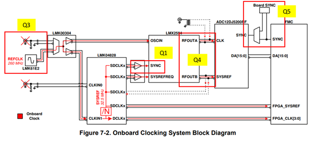
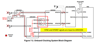
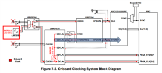
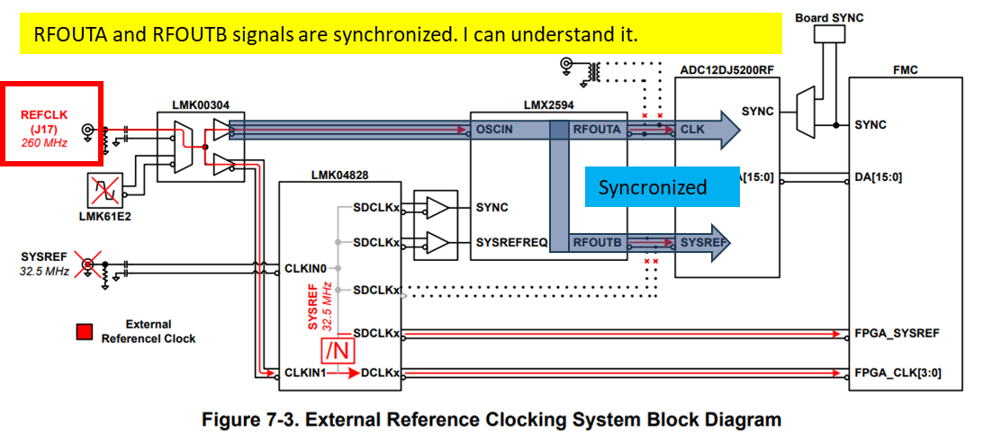
Q1. I consider that the SYNC signal input from the LMK04828 to the LMX2594 is used to align the output signals of multiple LMX2594 devices. (Fig7-2)
In the EVM diagram, there is only one LMX2594, so there is no need to input the SYNC signal, right?
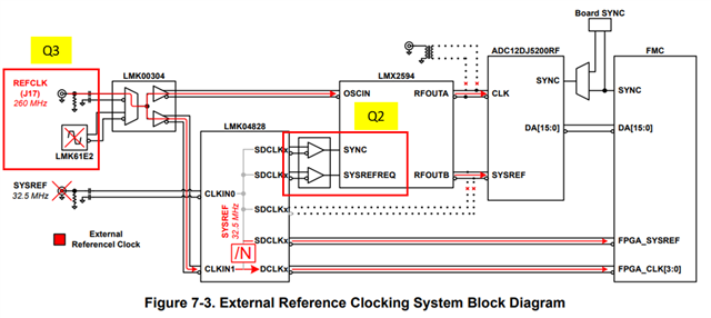
Q2. When using the Onboard Clocking System(Fig 7-2), the SYNC signal and SYSREFREQ signal are input from LMK04828 to LMX2594.
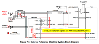
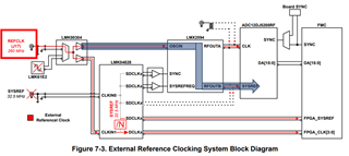
But, why are the SYNC and REFSYSREQ signals not input in the External Reference Clocking System(Fig 7-3)?
Q3. Why does the origin of SYSREF change just by changing the input source?
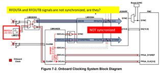
Q4. I believe that the LMX2594 outputs RFOUTA and RFOUTB need to be synchronized.
The External Reference Clocking System is satisfied because RFOUTA and RFOUTB are generated from OSCIN.
How does Onboard Clocking System synchronize?
Q5. What is Board SYNC?
Is it different from the SYNC~ sent from the RX side of JESD204?