This thread has been locked.

If you have a related question, please click the "Ask a related question" button in the top right corner. The newly created question will be automatically linked to this question.

ADS1282: Noise Floor is too large

Part Number: ADS1282

Tool/software:

Hello,


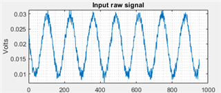
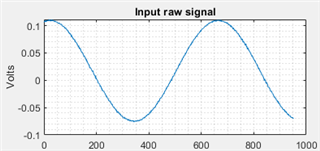
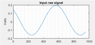
We are using ADS1282 and would like to estimate base line (noise floor) and having issues with output data.


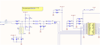
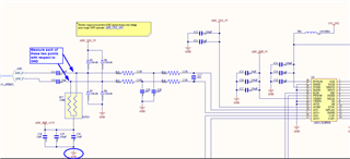
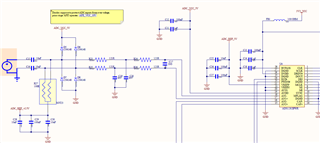
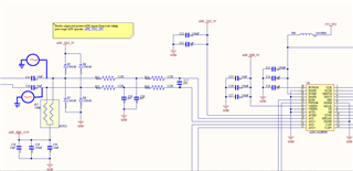
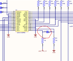
Hardwire configuration:


ADC reference set to 5V DC

AIN1+, AIN1- is connected via 121R to 2.5V reference voltage

ADC clock set at 4.096MHZ


Software Configuration

Config 0 register is configured to  0xD9


D7                           1             continuums SYNC mode

 D6                           1            reserved

 D5:D3                    001         64KHZ   data rate              Table6 page 18

 D2                           0            Linear phase

 D1: D0                   01           Sinc Filter is selected


Other registers left at default state


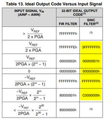
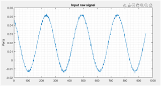
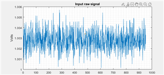
When reading 32 bit data , we expecting data to be near 0 , according to the table 13 page 26 data sheet,

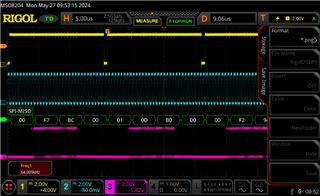
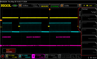
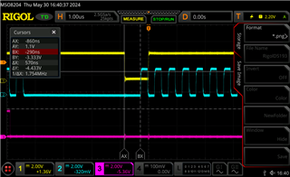
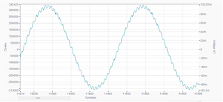
but we are getting relatively large noise floor, please see attached scope plot. Yellow line is ADC RDY ; blue SPI CLK; magenta is SPI Data Out from ADC.


Could you please advise what can be wrong?


Thank you,


Iouri

  • Hi louri Markin,

    Today is a holiday in the US, we will respond to your post later this week. Thanks for your patience

    -Bryan

  • Hello Iouri,

    I think your timing is incorrect.  You are reading the last LSBs of data less than 4 CLK cycles before the next /DRDY goes low, which will corrupt the next reading.

    Since you want to operate at 64ksps, and the maximum SCLK is 2.048MHz when using a CLK of 4.096MHz, you do not have enough time to read 32b and meet the 4 t-CLK periods before the next /DRDY falling edge.  In this case, I suggest you only read 24b (more than enough at these higher data rates).

    The process should follow below:

    1.  With SCLK idle LOW, the host MCU monitors for a falling edge on /DRDY (either through polling or interrupt).

    2.  After /DRDY goes low, delay 100ns or more, and then send 24 SCLKs (f-SCLK=2.048MHz), with the host capturing data on the SCLK rising edge.  The falling edge will shift the next bit out of the ADC.

    3.  After capturing the 24b word, idle SCLK LOW until the next falling edge of /DRDY and repeat steps 1-3.

    Regards,
    Keith Nicholas
    Precision ADC Applications

  • Hi Keith,

    Thank you for the reply, let me try and I will advise

    Regards,

    Iouri

  • Hi Keith,

    Thank you again for detailed reply. I have modify the code to accomplish 24 bit and 100 nS delay between filing edge of ADC RDY and rise of SCK.

    Please see scope plots below and comment.

    To do ADC counts to volts conversation I am using follow formula:

    <VOLTS > = 0.5 * 5V / (2^23 - 1) * <COUNTS>, I am assuming MSB is sign bit. 
    Please advise if this formula making sense.
    Thank you for your support.
    Iouri

  • Hello Iouri,

    Since you are using the SINC filter, the 24b code is divided by 2.

    With PGA=1:

    <VOLTS > = 0.5 * 5V / (2^22 - 1) * <COUNTS> ; for a 24b signed integer

    <COUNTS> is the decimal equivalent (signed integer) of the two's complement code.

    Regards,
    Keith

  • Hi Keith,

    I have updated calculation formula and results doesnt look right.

    I have applied 250mV differential sine wave 250HZ V offset = 2.5V DC to AIN0 channel, I am getting relatively large DC bias from 0, as well amplitude doesnt seem right. Please see bellow

    schematic of the input stage:

    Please review and advise if something doesnt look right.

    Thank you for your support.

    Regards,

    Iouri

  • Hello Iouri,

    I suggest using an oscilloscope and measure each of the inputs with respect to system ground.

    I am not sure what is going on based on the data you provided, but we need to confirm that the input signal is correct.

    Regards,
    Keith

  • Hi Keith,

    Thank you , for your reply. I did check DC bias at each input it is 2.5V DC; and AC- component is 250mV pk-pk at each input (180 degree phase shift between input)

    Regards,

    Iouri

  • Hello Iouri,

    Please also measure directly at the ADC pins, AN1- and AN1+ to make sure the voltages are correct.  With no input signal, use a DMM to measure the AN1- and AN1+ DC levels (both with respect to ground and differential, (AN1+)-(AN1-), to confirm near 0V.

    Also, without any AC input signal, record several readings to confirm the DC offset is near 0V.  The 100kOhm resistors and the 1N4148 diode leakage may be causing a DC shift.

    Finally, please include the raw output codes from the ADS1282 in a text file.  This will allow me to confirm you are using the correct math to convert to voltage.

    Thanks,

    Keith 

  • Hi Keith,

    Thank you for your replay. I did measure voltage from C17 (see schematic above, C17 is directly connected to ADC) pins to GND.

    measurements done with and without AC signal, using DMM . in both cases I am getting 2.481V  DC on both inputs. 

    Please also find raw (no AC signal data) data, this is 32 bit data ADC data D23: D0 is mapped to D31: D8 and D7:0 padded with 0.

    reason  I did this is to keep sign bit at MSB location , which makes easy to manipulate with negative numbers.

    Regards,

    Iouri

    putty_d1.log

  • Hello Iouri,

    Your data you provide looks like there is about 20mV offset.  This is probably due to leakage current from the protection diodes flowing through the 100kOhm bias resistor.

    As another test, please apply a 3.5V input to the positive input ( at R25/D6/D8 node ) with nothing connected to the capacitor inputs.  This should provide a 1V differential bias to the ADC inputs (An1+=3.5V, An1-=2.5V) and record several values.  The input code should show close to 1V.

    Also, I calculated the input voltage using the following expression.

    Vin = Code*2.5/(2^30-1)

    Vin = 8343040*2.5/(2^30-1) = 0.0194V.

    Regards,
    Keith

  • Hi Keith,

    Thank you very match for your reply

    1. apply 3.5V DC to AIN1+;

    2. measured with DMM differential voltage 994mV. 

    3. collect and plot data seems to be OK;

    Please see bellow 

    I still having problem when apply AC signal and getting wrong amplitude values, any advise here

    Thank you for all your support.

    Regards,

    Iouri

  • Hello Iouri,

    This looks correct.  At this point, there must be something not working as intended with the function generator.  

    I configured the ADS1282EVM with very similar setup as yours and do not see any issues.  Please note that I do not have the signal generator AC coupled; it is direct connected, differential output (200mVpp) with a 2.5V common mode.

    Maybe provide a connection diagram showing how your function generator is connected to the ADC inputs.

    Regards,
    Keith

  • Hi Keith,

    Thank you for your reply. We are using Rigol DG992 functional generator.  Generator has 2 channel output with ability to sync channels to generate differential signal. Generator CH1 is connected directly to ADC_N (C15) and GND; CH2 is connected to GND and ADC_P (C16).

     I did few more measurements, please see bellow.

    Few comments

    DC bias set to 2.5V  on both channel.  

      amplitude measurements done using scope across C17

    Please review and comment 

    Regards,

    Iouri

    100HZ  680mV Differential Voltage


    250HZ 680mV

    500HZ 660mV

  • Hello Iouri,

    Since you can set a 2.5V offset on each of the generator output channels, I suggest connecting on the other side of the capacitors C15/C16 to eliminate the AC coupling.  This will then be very similar to the tests that I did on the EVM.

    The ADC may also be damaged and need replaced.

    Regards,
    Keith

  • Hi Keith,

    Thank you for your reply.

    I have remove C15, C16 and applied signal from generator (100 HZ 680mV differential; 2.5V DC bias on each channel)  directly to R23, R25; result are bellow,

    please note Amplitude mentioned bellow are measurements taking across C17 :

    change, amplitude to 1100mV

    Thank you for all your support!!!!

    Regards,

    Iouri

  • Hello Iouri,

    I do not have any other suggestions at this time.  It appears you are getting a good signal, but the scaling is incorrect.  I would suggest replacing the ADS1282, but the DC measurement of 1V was the correct value.

    Regards,
    Keith

  • Hi Keith,

    Thank you for your reply. Let me try to get another board and I will advise in few days

    Regards,

    Iouri

  • Hi Iouri,

    O.K.

    Keith

  • Hi Keith,

    it looks my problem related to the amplitude was value of the capacitor connected to to pins CAP+ and CAP-, I think value what I am using seems to be too high,  see screenshot bellow. I change it to 10nF and remove R33 and R28 and it helps with frequency respond..

    Can you please comment on this? Also if there are any specification related to high/low cut frequency (-3dB) ?

    Please advise at your earliest convenience .

    Thank you for all your support.

    Regards,

    Iouri

  • Hello Iouri,

    Yes, 100nF will effect the bandwidth of the ADC input, and the resistors will further attenuate the signal. 100nF differential capacitor will result in a 3dB bandwidth of 2.6kHz.  If you had used a higher capacitor value, this would definitely attenuate the signal at 250Hz.

    Regards,
    Keith

  • Hi Keith,

    I think I am good for now. Thank you for your support

    Regards,

    Iouri