This thread has been locked.

If you have a related question, please click the "Ask a related question" button in the top right corner. The newly created question will be automatically linked to this question.

PGA 280 SPI driver.

Other Parts Discussed in Thread: PGA280, ADS1259

 Hello,


I am using PGA 280 with ADS1259 in our application. I was going to proceed with writing an SPI driver in C  for both of them starting with PGA 280. Apart from the application note for SPI are there any libraries in C available  for PGA280 ? 


Regards

Rahul

  • Hi Rahul,

    We'll look around and see if we've got anything to share with you.  What host processor do you plan to use here?

  • Hello Rahul,

    The software we have available on the PGA280 and ADS1259 is the EVM-PDK firmware.  This could not be considered a software library, just an example.  I could send it to you directly via email.

    Best Regards,

    Luis 

  • Hi Tom,

    We will be using STM32F103. It is a microcontroller by ST  and has an  ARM Cortex M3 core. Thanks for helping me out. I will be looking forward to your reply.


    Regards

    Rahul

  • Hi Luis,


    I was expecting your reply :) Yes please do send me the firmware, I will take the reference of that firmware to build my code for PGA. I have learnt a great deal about analog electronics after fiddling around with PGA so I would like to thank you for all your help you provided.


    Regards

    Rahul

  • Hello Rahul,

    Apologize for the delay.  Please find attached.

    Thank you and Best Regards,

    Luis

    8867.ADS1259_fw.zip

  • Hi Luis,


    I have a query regarding calculation of checksum of PGA280. During a read access to PGA 4 bytes will be sent to PGA which are command(command and address) + checksum byte + 2 dummy bytes . I will be recieving the data and checksum byte during the 2 dummy byte cycles. The datasheet does not state how a checksum byte is calculated during read access to PGA. It has been mentioned that for a write access checksum = 0x9h + command byte + data byte. Since for a read access i have no data to send then how should I calculate the checksum that i need to send to the PGA? When i receive a checksum from PGA during read access what is the procedure to verify checksum and decide the integrity of recieved data? Also why is the "mod" used in the calculation of checksum in the 1st example? I have copied the example below.

    Examples:
    0x4101DD Send Reset [CHKsum calculation: (0x9B + 0x41 + 0x01) mod 0x100 = 0xDD]


    Please can you also tell me the procedure to verify checksum from ADS1259 too?


    Regards

    Rahul

  • Hi Rahul,

    On the first question:

    During the Read command, when the device is set in CheckSum mode, the command structure is

    Read command to device = Command byte + CHKsum byte

    The Checksumbyte during the read command is  simply:

    CHKsum = (polynomial value + command byte) mod 0x100);

    where the polynomial value is 0x9B in hex coding, and the "mod" operation is used to remove the carry.

    Example:

    Read register 4:

    first byte: Command byte and address; second byte: Checksum byte;  dummy byte; dummy byte.

    Checksum:  ((0x9B +0x84) mod 0x100) = ((0x11F) mod 0x100) =  0x1F Note:  The modulus operation is used to ignore the carry; so the CHKsum is only 0x1F

    So you would send: 0x841F0000.

    Question:  When i receive a checksum from PGA during read access what is the procedure to verify checksum and decide the integrity of recieved data?

    Yes, the procedure is to compare the data received vs the checksum received; where the response is:

    Data byte + CHKsum byte

    where CHKsum = polynomial value + command byte + Data byte received.

    Question: Why is the "mod" used in the calculation of checksum in the 1st example? I have copied the example below.
    0x4101DD Send Reset [CHKsum calculation: (0x9B + 0x41 + 0x01) mod 0x100 = 0xDD]

    The modulus operation is used to remove the carry.  In this example, the result of the sum is 0xDD without a carry, but the datasheet is just emphasizing that the checksum is only one byte and the carry is ignored.

    Question: can you also tell me the procedure to verify checksum from ADS1259 too?

    In the extended SPI mode, if connecting through the PGA280 to the ADS1259; the ADS1259 provides its own checksum.  On the ADS1259 the checksum operation applies only to the readback operation of data; the checksum is given by:

    Checksum = MSB data byte + Mid Data byte + LSB data byte + 9Bh;

    Therefore the optional checksum is appended to the 3 conversion data bytes; and makes the data word length 4 bytes.  This is explained in detail on the ADS1259 datasheet page 29.

    Thank you and Best Regards,

    Luis 


  • Hello Rahul,

    The application note below gives more examples regarding the PGA280 SPI commands and functions...

    Best Regards,

    Luis

    http://www.ti.com/lit/an/sboa119/sboa119.pdf

  • Hi Luis,


    I understood how PGA checksum will be calculated. Correct me if i am wrong. During read access i will send checksum + comm + 2 dummy bytes. The calculation of checksum will be CHKsum = (polynomial value + command byte) mod 0x100);When i recieve checksum from PGA the caluculation of checksum to verify data integrity will be

    CHKsum_receive = (polynomial value + command byte+ data byte) mod 0x100); If the received checksum is equal to calculated CHKsum_receive then the data is correct.


    Regarding ADS1259: Checksum = MSB data byte + Mid Data byte + LSB data byte + 9Bh;

    But checksum is 1 byte data in ADS1259. Hence if the 24 bit data is all '1s' then checksum = 0xff +0xff +0xff +0x9bh which goes beyond one byte. Is the same rule for PGA applicable to ADC too? If not then how does ADS1259 calculate checksum and how do I verify it at microcontroller end?


    Regards

    Rahul

  • Hi Rahul,

    - On the first question about the PGA280 read data checksum, yes you are correct.

    - On the ADS1259 checksum question, you are correct,  the checksum is 8 bit in length and if the sum exceeds 0xFF, it will over flow, ignoring the carry and have only the Least significant bit. 

    check sum = MSB byte + Middle byte + LSB byte + 0x9Bh.

    The only exception is described on the datasheet: if the out-of-range FLAG is turned on, the check-sum byte is only 7 bit length; the 8 bit is replaced with the over-range flag; as shown on table 17 p29 of the datasheet.  The checksum carry above 7 bit  is ignored in this case, and you are left with the 7 least significant bits of the checksum.

    The over-of-range flag is a different function that detects if an input over-range has occured; where the differential input voltage VIN = AINP-AINN of the converter has exceeded the difference VREF= VREFP-VREFN.  If the diferential input exceeds +/-105% of FSR the flag will turn on.  This function is explained on page 14 of the datasheet.

    Regards,

    Luis


  •  


     Hi Luis,

    Thanks for your earlier reply. I am not able to interpret the datasheet correctly. I have few more queries about ADS1259


    1. After the DRDY goes low, there are two ways to read conversion data which are Data Read in Continuous mode and data read in Data Read in Stop Continuous mode. If I decide to read conversion data in Stop Continuous mode only then I will have to send a SDATAC command while configuring ADS1259 after power on. Is this the right procedure to configure ADS1259 to output data in  Stop Continuous mode only and never in Continuous mode ?

    2. In Continuous mode I cant read or write data to registers unless i send the SDATAC command. However in Stop Continuous mode it is possible to read and write data to registers. For eg : in Continuous mode after DRDY goes low, and i send clocks and command(RREG) to read register data, the ADS1259 will return conversion data instead of register data. To read register data i will have to send the SDATAC command and then command and clocks to read register data. In stop continuous mode after DRDY goes low i can send clocks and command to read register data and then send RDATA command to read conversion data. Is my understanding right?

    3. In continuous mode if i pull chip select high without issuing the SDATAC command, then during the next read access(register read) will ADS1259 still be in continuous mode and send conversion data instead of register data?

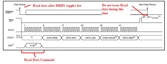
    4.What is the meaning of the following statement in datasheet Page 31 : "The read data command must be sent at least 20 f CLK cycles before the DRDY falling edge or the data are incorrect. Do not the read data command during this time". Is this the update time given on Page 30 in Fig 60?

    5. Is there any software guide on implementation of SPI of ADS1259?


    Will be looking forward to your reply.


    Regards

    Rahul


  • Hello Rahul,

    1. After the DRDY goes low, there are two ways to read conversion data which are Data Read in Continuous mode and data read in Data Read in Stop Continuous mode. If I decide to read conversion data in Stop Continuous mode only then I will have to send a SDATAC command while configuring ADS1259 after power on. Is this the right procedure to configure ADS1259 to output data in  Stop Continuous mode only and never in Continuous mode ?

    Yes, when you power up the device by default you are in the RDATAC mode.  You will need to send the SDATAC command if you wish to read data in the SDATAC Stop Data Continuous Mode  If you cycle the power or send a RESET command or assert the RESET pin, the device goes back to default settings and you are back in to the RDATAC mode.

    2. In Continuous mode I cant read or write data to registers unless i send the SDATAC command. However in Stop Continuous mode it is possible to read and write data to registers. For eg : in Continuous mode after DRDY goes low, and i send clocks and command(RREG) to read register data, the ADS1259 will return conversion data instead of register data. To read register data i will have to send the SDATAC command and then command and clocks to read register data. In stop continuous mode after DRDY goes low i can send clocks and command to read register data and then send RDATA command to read conversion data. Is my understanding right?

    On the ADS1259 the communication protocol is half duplex, meaning that data are transmitted to and from one direction at a time.  The RDATAC mode is cancelled by sending the SDATAC command.  This operation occurs simultaneaously with the ADC conversion data on DOUT which can be ignored in this case.  Once the SDATAC command has be sent then you can issue other commands such as WREG or RREG.  Yes, you are correct, in order to read registers you will need to send the SDATAC command in order to be able to send the RREG command.  You can send RDATA to read register conversion data while in the SDATAC mode of operation.  The only rule is that the RDATA command must be sent 20 fclk (oscillator clock cycles) before DRDY goes low. (more detail on question 4)

    3. In continuous mode if i pull chip select high without issuing the SDATAC command, then during the next read access(register read) will ADS1259 still be in continuous mode and send conversion data instead of register data?

    I don't think the RREG command works unless you are in the SDATAC mode of operation  The device is in RDATAC mode unless you send a SDATAC command. 

    4. What is the meaning of the following statement in datasheet Page 31 : "The read data command must be sent at least 20 f CLK cycles before the DRDY falling edge or the data are incorrect. Do not the read data command during this time". Is this the update time given on Page 30 in Fig 60?

    Yes, you are correct, during this time the internal conversion result register is updated during this time and data is being shifted; therefore, if you send RDATA command less than 20 fclk cycles before DRDY low, the data will be corrupt.  The procedure recommended is to monitor DRDY and send the RDATA command right after DRDY goes low to avoid this situation; or you may always go back to RDATAC mode after configuring the registers. 

    5. Is there any software guide on implementation of SPI of ADS1259?

    If I find anything with SPI examples for the ADS1259 I will update.. .  You may also search in the FORUM for previous questions users have posted. 

    Best Regards,

    Luis


  • Hi,

    I am trying to communicate with ADS1259 using PGA280 extended mode. I have successfully established SPI communication with PGA280. The chip select for ADS1259 using PGA GPIO extended mode pins is working fine. However the ADC is not responding at all.Here are a few of my observations:

    1. There is 0 volts on the bypass pin of ADS1259 when the ADS1259 is powered up. I compared this with the EVM of ADS1259. When the EVM board is powered up before connecting downloading the firmware the Bypass pin shows 0 volts too. After the firmware is downloaded the bypass pin shows the output of LDO which is 1.8 volts.Is there a specific set of commands or a specific power up sequence required for ADC?

    2. When the chip select of ADC goes high, the MISO should be tristated and since we have a pull up resistor the MISO line should be pulled high. However MISO line stays low all the time. This observation is with and without PGA in the circuit.


    Kindly reply as soon as possible

  • Hi,

    I resolved the issue which i posted above. It was related to a faulty resistor on the reset pin. Now the MISO line or Dout line of ADC goes high when ADC is deselected.


    Regards

    Rahul

  • Hi Rahul,

    Great news!  Thanks for letting us know.

  • Hi,


    In the earlier posts on the same thread I asked a question regarding the data to be collected from the ADC.

    What is the meaning of the following statement in datasheet Page 31 : "The read data command must be sent at least 20 f CLK cycles before the DRDY falling edge or the data are incorrect. Do not the read data command during this time". Is this the update time given on Page 30 in Fig 60?

    Your reply to this question was: Yes, you are correct, during this time the internal conversion result register is updated during this time and data is being shifted; therefore, if you send RDATA command less than 20 fclk cycles before DRDY low, the data will be corrupt.  The procedure recommended is to monitor DRDY and send the RDATA command right after DRDY goes low to avoid this situation; or you may always go back to RDATAC mode after configuring the registers. 


    However,apart from the grammatical error, dont you think the statement made in the datasheet and your reply contradict each other because the datasheet says that the read data command needs to be issued 20 fclk BEFORE the DRDY bit goes low. You are telling me to issue it after the DRDY bit goes low. I am using stop continuous mode to read data in Pulse conversion.


    I have one more query. Sometimes the ADS1259 takes too long to for the DRDY bit to go low after the start of conversion command is sent. Since the firmware has a dependency in ADC conversion, the firmware freezes too. Also sometimes the ADC does not respond for a long time and then suddenly it starts outputting values. Kindly help me out with this problem.Since I do not have more observations on this problem I apologize for not being able to explain the problem in details. PLease ask me any information you need.


    Regards

    Rahul

  • Hello Rahul,

    The data sheet specifies that new conversion data is available when DRDY goes low. DRDY is an output that indicates when the conversion data is available for reading.  

    When the device is running in Gate Control Mode (PULSE BIT =0, default) and the START pin is held high (or a START command is issued) the device starts performing one conversion after another. The data read operation must be completed 20 fclks before the next falling edge of the DRDY.  Therefore, in order to ensure that all data is read in the allowed time; the safest way to perform the read operation is to monitor the falling edge of the DRDY pin, and start the read of conversion data immediately after DRDY goes low. 

    On the Pulse Control Mode (Pulse Bit = 1); the device starts a single conversion when either the START pin is set high or when a START command is issued.  The DRDY goes high indicating the conversion has started, and DRDY toggles low when the conversion is completed; and the data is ready to be read.  The conversion results can be read immediately after the DRDY falling edge that indicates the conversion results are ready.

    Figure 61 shows STOP continuous mode below.


    - On the second question, I am not certain what is causing the DRDY to take too long to go low after the start conversion command is sent.  According to the description, you are using the Stop Continuous Mode and reading data on Pulse Control Mode (Pulse Bit =1).  I have a few questions about your current configuration:

    What is the sampling rate used? How long is the time for conversions to happen when the device does not respond?    

    I am assuming that START commands are being issued to control conversions.  Is this correct?  If using START commands to control the conversions, is the START pin held low? is Pulse Bit =1?  Are you monitoring the DRDY pin or polling the DRDY bit  in the CONFIG 2 register?

    Is the  RESET/PWDWN pin held high? Are you allowing 8 tclk cycles after a RESET high (or 2^16 tclk cycles when exiting a power-down) before communicating to the ADS1259?

    Any spikes or noise in the SCLK or RESET lines? The datasheet describes on page 28 that if an unintentional SCLK transition occurs from a noise spike, the device may not respond properly and the port can be reset by either: 1) toggling the CS pin high and then low; 2) holding SCLK low for 2^16 fclk cycles to reset the interface; 3) toggling the RESET pin low and high; or 4) cycling the power supplies. 

    If possible,  please send oscilloscope plots of the START, RESET, SCLK, DRDY, DOUT, DIN during a read operation.

    Thank you and Best Regards,

    Luis

  • Hi Luis,

    On your reply to the 1st question.  I am using 10 SPS, so I should get the DRDY falling edge or DRDY bit in CONFIG2 register goes low every 100 msec.(however I get the DRDY falling edge every 200 msec i.e it takes double the time for all SPS configurations, we can discuss this separately ) after the start command has been issued.I am currently polling the DRDY bit in CONFIG2 register. Hence in the software I will have to send a start command and wait till the DRDY bit is reset which will be 100msec wait time. During this time the processor will not do anything and only keep polling for the DRDY bit which is not acceptable.Another scheme that can be implemented is that the processor gives the start command and proceeds to do other task, and polls the DRDY bit only when it comes to the function block of reading ADC data . But then if the other tasks take more time than required it may happen that the DRDY bit is polled long time after the DRDY bit goes low. Hence the data will be incorrect..Right now my sequence of reading the data is that after i send the start command the state of the READ ADC DATA block is changed and the processor does other tasks and when it comes back to the READ ADC DATA block it checks whether EOC has been received by polling the DRDY bit.If EOC(end of conversion or data ready) is received then it goes ahead with reading the data. In this scheme i have a timeout implemented for DRDY which is of 400msec.Sometimes the DRDY bit gets polled at the wrong time consecutively resulting in a timeout condition This also could be the answer to the 2nd question i asked earlier,although I am not sure about it.  Anyway please can you tell me what is the best scheme to implement to read data from the ADC?

    The reset pwdn pin is held high permanently.There is no noise present on the lines now.


    Regards

    Rahul

  • Hello Rahul,

    If you have a free GPIO available, think it may be easier/more efficient to poll the DRDY pin instead of the DRDY bit; and to control the conversions with the START pin.  

    I am assuming you are using the START Pulse mode of operation with the PULSE bit set =1  (is this correct?).  The conversions should be ready after the the programmed "Initial START Delay" has passed and the digital filter has settled. Table 8 shows the DELAY[2:0] registers and corresponding delays in micro seconds.  Also refer to Table 9 (page 24), the conversion times after the START are dependent on the digital filter configuration.  For example, the conversion data is ready after 200ms when the device is set to 10SPS with fclk = 7.3728MHz, SINC2 filter and a Delay[2:0]=000  

    If you are controlling the conversions with the START pin (or command), the user should be able to read the results before sending the next START pulse to commence a new conversion.  The other issue to consider is to not to toggle the START pin during a conversion.

    After setting the configuration registers; are you able to read the conversion registers without issues? can you please confirm the configuration registers? What filter configuration is being used?

    Are you using the START pin to pulse the conversions or the START command? Please provide oscilloscope plots showing the CS, SCLK, DOUT, DIN, DRDY, START during a read conversion operation and a write Register operation.

    If possible, please provide an schematic showing the ADS1259-PGA280?

    Thank you,

    Best Regards,

    Luis