This thread has been locked.

If you have a related question, please click the "Ask a related question" button in the top right corner. The newly created question will be automatically linked to this question.

ADS8681: RVS not going high after reset

Part Number: ADS8681
Other Parts Discussed in Thread: ADS8685

Tool/software:

This is my first use of the device.  All grounds are connected to the same return plane. Upon initial power-up or reset (RST_n pin driven to 3.3V), the RVS pin remains low.  According to section 7.4.2.1 of the datasheet: "In order to exit any of the RESET states, the RST pin must be pulled high with CONVST/CS and SCLK held low. After a delay of tD_RST_POR or tD_RST_APP, the device enters ACQ state and the RVS pin goes high."  I read this to mean that CONVST/CS should remain low, along with SCLK until RVS goes high.  Please advise.

Please advise.  I am driving the device with an FPGA using 3.3V I/O.

DGND = 0V

AVDD = 5.2V

AGND = 0V

REFIO = ~4.09V

REFGND = 0V

REFCAP = ~4.09V

AIN_P = Unconnected

AIN_GND = 0V

RST_n = 0V or 3.3V

SDI = 0V

CONVST/CS_n = 0V (FPGA is waiting for RVS to go high before starting a conversion)

SCLK = 0V

SDO-0 = 0V when RST_n = 0V; 3.3V when RST_N = 3.3V

ALARM/SDO-1/GPO = 0V

RVS = 0V

DVDD = 3.3V

  • Hi Brent!

    Welcome to our e2e forum!  Can you provide a schematic and any timing screen shots (o'scope preferred, logic analyzer is OK) showing the control signals? That would be very helpful getting started with your issue.  Any detail you can provide on your register settings would also be helpful.

  •   

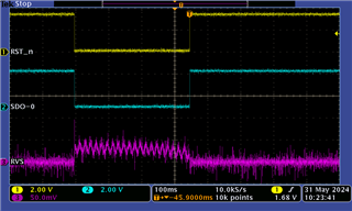
    4V_Ref and Ain are currently unconnected, and the digital signals are tied directly to the FPGA I/Os.  A correction to the voltages above is REFIO and REFCAP are 3.79V when RST_n is 0V and 4.09V when RST_n is 3.3V.  I have two of these circuits, with all digital signals connected individually to the FPGA I/Os (no shared pins or daisy chaining).  Both circuits yield the same results.  All other signals are constant during the transients, but note the voltage scaling on RVS:

  • With a 10k pull-up to 3.3V on RVS, its voltage goes to 3.3V when RST_n is 0V.  That would lead me to believe that RVS is open-drain. Is that expected?

  • Hi Brent,

    It's actually a driven digital output, it should not be an open-drain connection.  Can you get some of the other control lines?  /CS, SCLK, SDI etc?

  • I am actually using an ADS8685, but the issue is still appropriate.  I am able to read/write to the device as expected.  The RVS pin eventually goes high (to 3V3 without a pull-up), but only after /CS is held high for at least ~610 ns (after waiting 20 ms after reset).  I was expecting RVS go high ~20 ms after reset, and not have to drive \CS high first, as in Figure 6-2.

  • Happy to hear that you have it working!

  • RVS still does not go high after reset without driving \CS high.  If this is the intended operation, the datasheet is very misleading (Section 7.4.2.1 and Figure 6-2), as I was originally waiting for RVS to go high before driving any signals high. Are you able to reproduce my findings?  If so, I believe the datasheet needs corrected.

  • Hi Brent,

    Here is a screen shot with a low /RST pulse with CONVST/CS held high (SCLK is don't care) - RVS goes high ~1.4mS later:

    Here is another with CONVST/CS held low (SCLK is don't care) - RVS is always low:

    Here it is again, with CONVST/CS held low followed by the start of normal conversions by toggling CONVST/CS.  RVS goes high after ~1.4ms, followed by the behavior described in Figure 6-3. 

    The datasheet is being updated to reflect the proper behavior.

  • Thank you for the clarification.  I was mislead by the phrasing of "In order to exit any of the RESET states, the /RST pin must be pulled high with CONVST/CS and SCLK held low.", which I interpreted to mean CONVST/CS should be held low, but it appears it needs to be pull high before RVS will go high.  Please change the phrasing of this sentence (in section 7.4.2.1, RESET State), and include or note that CONVST/CS must be high in Figure 6-2.