This thread has been locked.

If you have a related question, please click the "Ask a related question" button in the top right corner. The newly created question will be automatically linked to this question.

ADC12QJ1600: Microchip Polarfire FPGA JESD204B configuration

Part Number: ADC12QJ1600

Tool/software:

Hi,

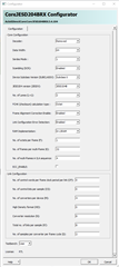
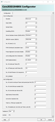
I would like to configure Microchips JESD204B core for PolarFire FPGAs together with the ADC12QJ1600 ADC.

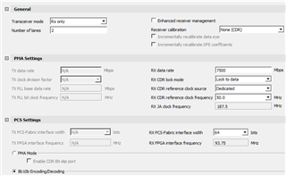
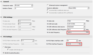
A limitation in hardware is that I only have a maximum of 4 lanes connected to the FPGA.

First step is to setup the ADC with only one core (A) enabled and the other cores (B, C, D) powered down.

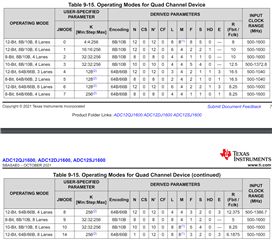
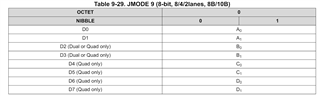
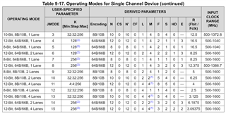
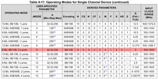
If I select JMODE9 (8-bit, 2 lanes, 8B/10B encoding), how should I configure the FPGA JESD core?

/Mikael

  • Hello Mikael,

    Please look in the ADC datasheet for details on the JESD mode parameters see table 9-15, these will give you all the parameters to fill in to this gui you are showing.

    Also table 9-29 will show you how the data gets packed across the JESD lanes

    Additionally, if you only have 4 lanes available the ADC has JMODEs that will support all channels across 4 lanes.

    Best,


    Eric

  • Hi,

    Thank you for your response.

    The thing is, I have the quad device, but to start with I only want to use the first core (A). The other cores will be powered down.

    So I will only connect the first two lanes.

    Is this still achievable with JMODE9? or do I have to connect all 8 lanes to get that mode working?

    /MIkael

  • Hello Mikael,

    This is not a problem, the ADC will work in this mode. To enable this you will have to enable the "SINGLE_CH_EN" register in the ADC reg 0x209, and from a JESD standpoint your configuration will be slightly different as the number of lanes changed. In the ADC datasheet there is a section discussing the JESD configuration for just a single channel of the ADC. Please see table 9-17 (screenshot below) in this you will see JMODE9 is very similar but now it is just for a single channel of the ADC and only uses two lanes. Please use these JESD parameters to configure your FPGA.

    best,

    Eric

  • Hi,

    So I configured the ADC for single core according to your suggestions.

    and the FPGA core according to the following:

    Sampling frequency 1500MHz based on a 50MHz XO on SE_CLK and PLLREFO outputs to supply the FPGA with the same reference clock.
    Sync pin is used for synchronization.
    SYSREF and TMSTP inputs unused.

    Device is setup according to the sequence defined in the datasheet section 10.3.

    I'm monitoring the SYNCSE signal which is generated by the FPGA core, which I expected to toggle LOW then HIGH, but it is stuck low.

    Some status register readouts from the ADC (let me know if you would like to see others):

    JESD_STATUS (0x208) - 0x01
    INIT_STATUS (0x270) - 0x01
    VCO_CAL_STATUS (0x5E) - 0x03
    CAL_STATUS (0x6A) - 0x0C
    ALARM_STATUS (0x2C1) - 0x08 (after clearing bits at startup)

    Looks like it is not able to pass the synchronization step??
    Why isn't SPLL_LOCKED active? Isn't it based on CPLL which is locked according to JESD_STATUS register?

    Thanks!

    Best Regards

    Mikael

  • Hello Mikael,

    Can you confirm if you are using the ADC EVM or a custom board?

    Yes the SPLL should lock, it is derived from the device clock which in this case comes from the CPLL. Before programming the FPGA are you able to read the value of the JESD_STATUS register (0x208).

    Another problem you will run into is that the clocks output form the ADC to the FPGA might be a different frequency then your FW is expecting, can you share what you XCVR Ref clock should be as well as what the JESD Core clock should be? Either of these being incorrect would cause the link to hang.

    Thanks,

    Eric

  • Can you confirm if you are using the ADC EVM or a custom board?

    It is a custom board.

    Yes the SPLL should lock, it is derived from the device clock which in this case comes from the CPLL. Before programming the FPGA are you able to read the value of the JESD_STATUS register (0x208).

    ADC device pins:

    PD - HIGH (device is powered up)
    PLL_EN - HIGH
    PLLREF_SE - HIGH
    SYNCSE - LOW
    CALTRIG - LOW
    CLKCFG[0..1] - LOW

    Reading JESD_STATUS before any ADC SPI configuration (FPGA is still programmed):

    JESD_STATUS (0x208) - 0x05

    so is there any problems with my SPI config perhaps (since the SPLL is locked at power up)?

    Another problem you will run into is that the clocks output form the ADC to the FPGA might be a different frequency then your FW is expecting, can you share what you XCVR Ref clock should be as well as what the JESD Core clock should be? Either of these being incorrect would cause the link to hang.

    I posted the configuration page for the transceiver core below:

    /Mikael

  • Hello Mikael,

    A JESD_STATUS of 0x05 is good it indicates that both the cpll and spll are locking, but it also indicates that the sync of the ADC is being held low which points to an FPGA FW issue.

    Your issue looks to me that the clocks are being set to serdes/80 for the RX fabric clock and serdes/40 for the RX JA clock. Can you confirm how you are generating the clock these reference clocks to the FPGA. My guess is that these are wrong.

    Best,

    Eric

  • A JESD_STATUS of 0x05 is good it indicates that both the cpll and spll are locking, but it also indicates that the sync of the ADC is being held low which points to an FPGA FW issue.

    This is a misunderstanding.

    The JESD status is still 0x01, so S-PLL is NOT locked, only C-PLL.

    This is a mystery to me! I cannot see why the S-PLL lock would fail?

    Your issue looks to me that the clocks are being set to serdes/80 for the RX fabric clock and serdes/40 for the RX JA clock. Can you confirm how you are generating the clock these reference clocks to the FPGA. My guess is that these are wrong.

    I'm using the SE_CLK input with a 50 MHz XO.

    It is used as a reference to the C_PLL to generate the 7500 MHz sampling clock.

    The 50 MHz XO is also routed to the FPGA via PLLREFO outputs and used as a the "RX CDR reference clock" in the FPGA IP core config.

    FPGA IP core settings:

    The "RX JA clock frequency" is automatically calculated based on the "RX data rate" set to 7500.

    Does the "RX JA clock frequency" have to match the "RX FPGA interface frequency"? I think not?

    Regards

    Mikael

  • Hello Mikael,

    The SPLL should be locked if you just bring up the ADC without the FPGA you should see this happen. If the Link fails to come up this will also be low.

    I am not sure what you mean by generating a 7500 MHz sampling clock, I believe you are referencing the vco inside the part. This is divided down to the actual clock rate of the part, which has a max of 1.6 GHz

    Your RX data rate should be the line rate of the serdes link which in this mode can be calculated as Fs*R.

    Your other two clocks serve different purposes. One will be used as a reference clock to lock the pll inside the FPGA to the line rate of the link and the other will serve as the JESD core clock. I am unfamiliar with how the microfire IP is configured and designed to work so you will have to follow up with them to know exactly what the ratios should be. Typically some default values for the core clock are Line rate/40 or line rate/80 for 8b10b modes.

    Best,

    Eric

  • Hi,

    I managed to get it working. It was a ADC configuration problem with the initialization.

    Thanks for the support!