Tool/software:
Hello,
I am using ADS7066 as a SPI slave in single mode. Can you please help with the following question, suppose if I do below steps.
>> Sending bytes through SDI
>> Getting output from SDO
Steps:
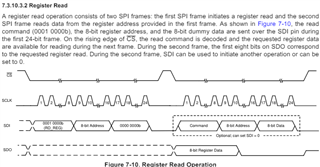
1. I sent \x08\x04\x04 (3 bytes) to set the OP_MODE_CFG Register to Value 4.
2. Then, I send \x10\x04\x00 to read the register, I get random 3 bytes, (First READ) = \x00\x0E\x00
3. Now, if I send \x10\x04\x00, I now get the read data which says \x04\x00\x00 (implies set) (Second READ)
Question:
Why the first READ REGISTER after WRITE is not functioning, why is it functioning from the second READ??
//Snippet
write_to_spi_device(): Write_command: [<ADS7066_OpCode.WREG: 8>, <ADS7066_Register.OPMODE_CFG: 4>, <ADS7066_ClockDivider.CLK_DIV_4: 4>], read_result_values: {0: 2, 1: 0, 2: 0} = \x02\x00\x00
read_from_spi_device(): Read_command: [<ADS7066_OpCode.RREG: 16>, <ADS7066_Register.OPMODE_CFG: 4>, <ADS7066_OpCode.NULL: 0>], read_result_values: {0: 0, 1: 14, 2: 0} = \x00\x0E\x00
read_from_spi_device(): Read_command: [<ADS7066_OpCode.RREG: 16>, <ADS7066_Register.OPMODE_CFG: 4>, <ADS7066_OpCode.NULL: 0>], read_result_values: {0: 4, 1: 0, 2: 0} = \x04\x00\x00
Note: I am using Ni8452 as a SPI master in the single mode with the below configurations to connect to SPI slave
// NI845x slave device connect configurations
ni845x_spi.set_ni845x_spi_configurations(
chip_select = dev_types.ni845x_types.ChipSelect.CHIP_SELECT_0, # Chip Select chosen for the SPI slave device
sclk_rate = dev_types.ni845x_types.ClockRate.CLK_10000, # Deafult = 10MHz
sclk_rate_polarity = dev_types.ni845x_types.Cpol.kNi845xSpiClockPolarityIdleLow, # Default = LOW
sclk_phase = dev_types.ni845x_types.Cpha.kNi845xSpiClockPhaseFirstEdge, # DEFAULT = First Edge
bits_per_sample = 8, # ADS7066 sample size = 8bits
port = 0 # Port 0 to 7 as 8 devices can be connected in Single Standard Mode
)
Does sample size being set to 8 has anything to do with this behaviour from ADS7066??
Regards
Sai Satwik Vaddi
Developer