This thread has been locked.

If you have a related question, please click the "Ask a related question" button in the top right corner. The newly created question will be automatically linked to this question.

ADC34J45EVM: T10 in schematic and PCB has not the intended functionality.

Part Number: ADC34J45EVM

Tool/software:

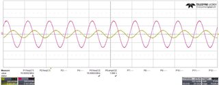
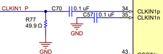
The T10 used for an external reference clock was intended as follows:

However, what you soldered was the Minicircuit part TC1-1-13M+

Which has following connection:

In order to get the functionality as shown in the schematic the transformer has to be turned.

  • Hi Goran,

    This is a balun and not a transformer. It is being used as intended as the pin out is correct, it is just the coils on the schematic symbol is wrong and looks like a traditional transformer. Baluns offer better load balancing for the downstream P/N signals. The signals are both AC coupled after the balun termination resistor so there is no issues with this schematic.

    Chase

  • Hello Chase,

    When I connect a DC free 10 MHz reference clock to J10 and connect 2 Lecroy probes of type PP007-WR to a LeCroy WavePro 735Zi-A- scope and measure the P and N at the resistor R85 I see:

    The signals are shifted -> phase error and the amplitude is about halve -> amplitude error. Do you agree that this is somehow wrong?

    When you fix the schematic of the transformer and replace it by balun... can you as well fix the capacitors R73 and R80 which are of schematic type resistor but with 0.1 uF capacitors equipped... this for clarity reasons. People tend to get confused when a resistor has the value 100nF :-)

    Then the resistor R40 has a very low value and we were not able to lock the PLL1 on the 10 MHz... we simply removed the resistor to make the PLL1 lock.

    Cheers

    Goran

  • Goran,

    Yes, that seems a bit extreme for phase and amplitude imbalance. I don't think we'll be updating the schematic any time soon but I've taken note of the schematic change request and will see they are implemented if/when board is redone. You can also drive the LMK with a single ended, AC coupled input by depopulating R85, C72 and populating R81, R46 and C33. This is what I do on new board designs, see below. The CLKin1 input comes from an SMA input and is AC coupled before it hits the CLKIN1_P net below.

    Thanks, Chase

  • Hello Chase,

    Did your PLL1 lock without removing R40???? I'd be very surprised. Please note: If PLL1 does not lock, but drives the VCO to the extreme frequency (VCO input basically at 3.3V) then the PLL2 will multiply this wrong frequency and your ADC will be operated not at the intended rate but by a wrong one.

    Cheers
    Goran

  • Hi Goran,

    No, the PLL won't lock on this board unless it is removed. 24Ω is too agressive of a pullup, and isn't even required.. For the LMK048xx devices, PLL1 will provide the charge pump current to lock the VCXO. I don't know how this EVM was designed 10 yrs ago but I suspect it was meant to be a place holder and the bom was incorrectly showing to install this resistor.

    Thanks, Chase

  • Hello Chase,

    I wonder how much time it consumes at the customers side and at the TI support side by helping the customers with a known error... just removing the R40 might be simpler for us all... instead of managing an error for 10 years.

    Cheers
    Goran