This thread has been locked.

If you have a related question, please click the "Ask a related question" button in the top right corner. The newly created question will be automatically linked to this question.

ADS131M08EVM: Reading data -- Connection issue?

Part Number: ADS131M08EVM
Other Parts Discussed in Thread: MSP432E401Y, ADS131M08

Tool/software:

Hi,

I am able to read, write and re-write any of the settings registers. So the SPI works (I have connected my EVM to a MSP432E401Y Launchpad). I am trying to apply a known signal from the function generator,

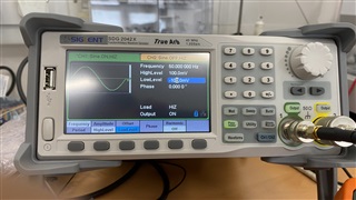
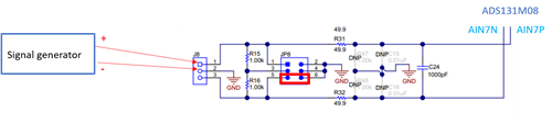
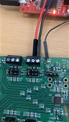
The +ve goes to the + side of J8 (I am using channel 7) and the gnd of the function generator is tied to the EVM and launchpad gnds and provided to the - of the J8. The JP8 jumper is in the default position (middle). Please see the attached image.

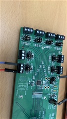
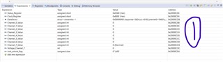
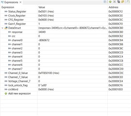
I have enabled channel7, and I can see it in the clock register (attached image).

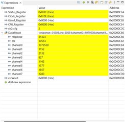
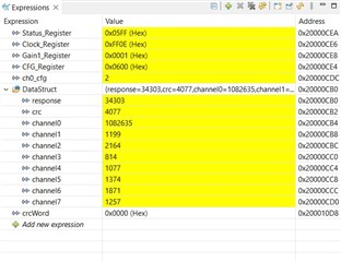
I don't get the correct data entry. Whatever I change the input, the value seems to be fixed. Is my jumper and connections settings correct? I even switched my jumper to JP8 [5-6], but I don't seem to read the data correctly.

Thanks

Ram.

  • Hi Ram,

    Your signal is a single-ended bipolar signal (-100mV~100mV), so the GND of your cable which is also the GND of your function generator should be connected to the GND of the EVM, not the - of the JP terminal block on the EVM board. The ADS131M08 ADC always converts the differential signal between AIN7P and AIN7N, the ADC can directly accept a negative input signal so you can install the jumper to the pin 5 and 6 of the J8 which will short AIN7N to the GND.  You can connect the function generator and configure the EVM according to the following block diagram. Let me know if you have any further questions.

    BR,

    Dale

  • Hi Dale,

    I made the connection as you said. But somehow, I am facing another problem. I was not able to read correct values, and found out that the clock and and cfg registers gets changed midway. May be some stray signal would. So I locked the registers after I set. The first image is the start of the debug, at line 92. The status and clock are set.

    I have my next breakpoint at line 97, and when I read, I get the values below, and as you see, the status shows that registers are LOCKED.

    After I read the values, I see this, a breakpoint at line 109.

    It seems it is a CRC error. The connections are provided as mentioned in your previous reply. Not sure where I am going wrong. Attaching the code for reference.

    /*
    
    1. Make all the hardware connections in the ADS board. SYNC/RESET, CS, DRDY, DIN, DOUT, AVDD, DVDD, GND. 
      
    2. This is a check code. There is a function called adcStartup(), in which one register is read back. 
      
    3. Ensure that the valuse read back is correct as per the datasheet and then proceed to have your code 
      written after this function. 
    
    The functions are referred from an existing code example from TI. 
    */
    
    
    //****************************************************************************
    //
    // LaunchPad pinout...
    //
    //****************************************************************************
    //
    //                  LEFT                                RIGHT
    //               /--------\                          /--------\
    //        +3.3V -|3V3  +5V|- +5V                CLK -|PG1  GND|- GND
    //              -|PD2  GND|- GND       nSYNC/nRESET -|PK4  PM7|-
    //              -|PP0  PB4|-                    nCS -|PK5 *PP5|-
    //              -|PP1  PB5|-                  nDRDY -|PM0  PA7|-
    //              -|PD4  PK0|-                        -|PM1  RST|-
    //              -|PD5  PK1|-                        -|PM2  PQ2|- DIN
    //         SCLK -|PQ0  PK2|-                        -|PH0  PQ3|- DOUT
    //              -|PP4* PK3|-                        -|PH1 *PP3|-
    //              -|PN5  PA4|-                        -|PK6  PQ1|-
    //              -|PN4  PA5|-                        -|PK7  PM6|-
    //               \--------/                          \--------/
    //


    #include <stdint.h>
    #include <stdbool.h>
    #include "ti/devices/msp432e4/driverlib/driverlib.h"
    #include "ads131m0x.h"
    
    uint32_t systemClock;
    uint16_t register_value, ID_Register, Status_Register, Mode_Register, Clock_Register, CFG_Register;
    uint32_t Channel_0_Value, Channel_1_Value, Channel_2_Value, Channel_3_Value, Channel_4_Value, Channel_5_Value, Channel_6_Value, Channel_7_Value;
    adc_channel_data *DataStruct;
    uint16_t crcWord = 0;
    int32_t Voltage_Channel_7;
    
    // Flag to indicate if a /DRDY interrupt has occurred
    static volatile bool flag_nDRDY_INTERRUPT = false;
    static volatile bool read_flag = false;
    static volatile bool lock_unlock_flag;
    #define SSI_BASE_ADDR       (SSI3_BASE)
    
    //*****************************************************************************
    //
    // The error routine that is called if the driver library encounters an error.
    //
    //*****************************************************************************
    #ifdef DEBUG
    void
    __error__(char *pcFilename, uint32_t ui32Line)
    {
        while(1);
    }
    #endif
    
    //*****************************************************************************
    //
    // Main Function. All other functions are written down
    //
    //*****************************************************************************
    int main(void)
    {
        // IMPORTANT: Make sure device is powered before setting GPIOs pins to HIGH state.
    
        // Initialize GPIOs pins used by ADS131M0x
        InitGPIO();
    
        // Initialize SPI peripheral used by ADS131M0x
        InitSPI();
        // Run ADC startup function
    
        while(1)
        {
            adcStartup();
            writeSingleRegister(CLOCK_ADDRESS, 0x800E);
            delay_ms(10);
            Clock_Register = readSingleRegister(CLOCK_ADDRESS);
            delay_ms(10);
            Status_Register = readSingleRegister(STATUS_ADDRESS);
            delay_ms(10);
            lock_unlock_flag = lockRegisters();
            delay_ms(10);
            Status_Register = readSingleRegister(STATUS_ADDRESS);
            delay_ms(10);
            read_flag = readData(&DataStruct);
            lock_unlock_flag = unlockRegisters();
            delay_ms(10);
            Status_Register = readSingleRegister(STATUS_ADDRESS);
            delay_ms(10);
            Clock_Register = readSingleRegister(CLOCK_ADDRESS);
            delay_ms(10);
            // Initialize SPI peripheral used by ADS131M0x
            InitSPI();
            adcStartup();
            delay_ms(10000);
            Voltage_Channel_7 = (((Channel_7_Value*3.3)/16777216)*1000);
            delay_ms(90000);
            delay_ms(10000);
            delay_ms(90000);
        }
    
    }
    
    //*****************************************************************************
    //
    //! Configures the MCU's GPIO pins that interface with the ADC.
    //!
    //! \fn void InitGPIO(void)
    //!
    //! \return None.
    //
    //*****************************************************************************
    void InitGPIO(void)
    {
    
        /* Enable the clock to the GPIO Port K and wait for it to be ready */
        MAP_SysCtlPeripheralEnable(SYSCTL_PERIPH_GPIOK);
        while(!(SysCtlPeripheralReady(SYSCTL_PERIPH_GPIOK)))
        {
        }
    
        /* Configure the GPIO for 'nSYNC_nRESET' as output and set high */
        MAP_GPIOPinTypeGPIOOutput(nSYNC_nRESET_PORT, nSYNC_nRESET_PIN);
        MAP_GPIOPinWrite(nSYNC_nRESET_PORT, nSYNC_nRESET_PIN, nSYNC_nRESET_PIN);
    
        /* Configure the GPIO for 'nCS' as output and set high */
        MAP_GPIOPinTypeGPIOOutput(nCS_PORT, nCS_PIN);
        MAP_GPIOPinWrite(nCS_PORT, nCS_PIN, nCS_PIN);
    
        /* Enable the clock to the GPIO Port M and wait for it to be ready */
        MAP_SysCtlPeripheralEnable(SYSCTL_PERIPH_GPIOM);
        while(!(SysCtlPeripheralReady(SYSCTL_PERIPH_GPIOM)))
        {
        }
    
        /* Configure the GPIO for 'nDRDY' as input with falling edge interrupt */
        GPIOIntRegister(nDRDY_PORT, GPIO_DRDY_IRQHandler);
        MAP_GPIOPinTypeGPIOInput(nDRDY_PORT, nDRDY_PIN);
        MAP_GPIOIntTypeSet(nDRDY_PORT, nDRDY_PIN, GPIO_FALLING_EDGE);
        MAP_GPIOIntEnable(nDRDY_PORT, nDRDY_PIN);
        MAP_IntEnable(nDRDY_INT);
    }
    
    //*****************************************************************************
    //
    // Interrupt handler for nDRDY GPIO
    //
    //*****************************************************************************


    //*****************************************************************************
    //
    //! Interrupt handler for /DRDY falling edge interrupt.
    //!
    //! \fn void GPIO_DRDY_IRQHandler(void)
    //!
    //! \return None.
    //
    //*****************************************************************************
    void GPIO_DRDY_IRQHandler(void)
    {
    
        // Possible ways to handle this interrupt:
        // If you decide to read data here, you may want to disable other interrupts to avoid partial data reads.
    
        // In this example we set a flag and exit the interrupt routine. In the main program loop, your application can examine
        // all state flags and decide which state (operation) to perform next.
    
        /* Get the interrupt status from the GPIO and clear the status */
        uint32_t getIntStatus = MAP_GPIOIntStatus(nDRDY_PORT, true);
    
        /* Check if the nDRDY pin triggered the interrupt */
        if(getIntStatus & nDRDY_PIN)
        {
            /* Interrupt action: Set a flag */
            flag_nDRDY_INTERRUPT = true;
        }
    
        /* Clear interrupt */
        MAP_GPIOIntClear(nDRDY_PORT, getIntStatus);
    
        // NOTE: We add a short delay at the end to prevent re-entrance. Refer to E2E issue:
        // https://e2e.ti.com/support/microcontrollers/tiva_arm/f/908/p/332605/1786938#1786938
        SysCtlDelay(3);
    }
    
    //*****************************************************************************
    //
    //! Configures the MCU's SPI peripheral, for interfacing with the ADC.
    //!
    //! \fn void InitSPI(void)
    //!
    //! \return None.
    //
    //*****************************************************************************
    void InitSPI(void)
    {
        //
        // Enable the clock to SSI-3 module and configure the SSI Master
        //
        MAP_SysCtlPeripheralEnable(SYSCTL_PERIPH_SSI3);
        while(!(MAP_SysCtlPeripheralReady(SYSCTL_PERIPH_SSI3)))
        {
        }
    
        //
        // Enable clocks to GPIO Port Q and configure pins as SSI
        //
        MAP_SysCtlPeripheralEnable(SYSCTL_PERIPH_GPIOQ);
        while(!(MAP_SysCtlPeripheralReady(SYSCTL_PERIPH_GPIOQ)))
        {
        }
    
        MAP_GPIOPinConfigure(GPIO_PQ0_SSI3CLK);
        //MAP_GPIOPinConfigure(GPIO_PA3_SSI0FSS); // Using GPIO for nCS instead of the FSS pin.
        MAP_GPIOPinConfigure(GPIO_PQ2_SSI3XDAT0);
        MAP_GPIOPinConfigure(GPIO_PQ3_SSI3XDAT1);
        MAP_GPIOPinTypeSSI(GPIO_PORTQ_BASE, (GPIO_PIN_0 | GPIO_PIN_2 | GPIO_PIN_3));
    
        /* Configure the system clock for 120 MHz */
        systemClock = MAP_SysCtlClockFreqSet((SYSCTL_XTAL_25MHZ | SYSCTL_OSC_MAIN |
                                                  SYSCTL_USE_PLL | SYSCTL_CFG_VCO_480),
                                                  120000000);
    
        // Configure: SPI MODE 1, 5 MHz SCLK, 8-bits per frame
        MAP_SSIConfigSetExpClk(SSI_BASE_ADDR, systemClock, SSI_FRF_MOTO_MODE_1,   \
                               SSI_MODE_MASTER, (systemClock/24), 8);
        //MAP_SSIEnable(SSI_BASE_ADDR);
    
        //
        // Enable the SSI2 module.
        //
        SSIEnable(SSI_BASE_ADDR);
        SSIAdvModeSet(SSI_BASE_ADDR, SSI_ADV_MODE_READ_WRITE);
        SSIAdvFrameHoldDisable(SSI_BASE_ADDR);
    
        //
        // Read any residual data from the SSI port.  This makes sure the receive
        // FIFOs are empty, so we don't read any unwanted junk.  This is done here
        // because the SPI SSI mode is full-duplex, which allows you to send and
        // receive at the same time.  The SSIDataGetNonBlocking function returns
        // "true" when data was returned, and "false" when no data was returned.
        // The "non-blocking" function checks if there is any data in the receive
        // FIFO and does not "hang" if there isn't.
        //
        uint32_t junk;
        while(MAP_SSIDataGetNonBlocking(SSI_BASE_ADDR, &junk));
    }
    
    //*****************************************************************************
    //
    //! Start up sequence for the ADS131M0x.
    //!
    //! \fn void adcStartup(void)
    //!
    //! Before calling this function, the device must be powered,
    //! the SPI/GPIO pins of the MCU must have already been configured,
    //! and (if applicable) the external clock source should be provided to CLKIN.
    //!
    //! \return None.
    //
    //*****************************************************************************
    void adcStartup(void)
    {
        /* (OPTIONAL) Provide additional delay time for power supply settling */
    	delay_ms(50);
    	setCS(LOW);
    	delay_ms(2);
    	/* (REQUIRED) Set nRESET pin high for ADC operation */
    	setSYNC_RESET(HIGH);
    
    	/* (OPTIONAL) Toggle nRESET pin to ensure default register settings. */
    	/* NOTE: This also ensures that the device registers are unlocked.	 */
    	toggleRESET();
    
        /* (REQUIRED) Initialize internal 'registerMap' array with device default settings */
    	restoreRegisterDefaults();
    
        /* (OPTIONAL) Validate first response word when beginning SPI communication: (0xFF20 | CHANCNT) */
    	//uint16_t response = sendCommand(OPCODE_NULL);
    
    	/* (OPTIONAL) Define your initial register settings here */
        //writeSingleRegister(CLOCK_ADDRESS, (CLOCK_DEFAULT & ~CLOCK_OSR_MASK) | CLOCK_OSR_256);
    
        /* (REQUIRED) Configure MODE register settings
         * NOTE: This function call is required here for this particular code implementation to work.
         * This function will enforce the MODE register settings as selected in the 'ads131m0x.h' header file.
         */
       // writeSingleRegister(MODE_ADDRESS, MODE_DEFAULT);
    
        /* (OPTIONAL) Read back all registers */
    
    	/* (OPTIONAL) Check STATUS register for faults */
    }
    
    
    //*****************************************************************************
    //
    //! Provides a timing delay with 'ms' resolution.
    //!
    //! \fn void delay_ms(const uint32_t delay_time_ms)
    //!
    //! \param delay_time_ms is the number of milliseconds to delay.
    //!
    //! \return None.
    //
    //*****************************************************************************
    void delay_ms(const uint32_t delay_time_ms)
    {
        const uint32_t cycles_per_loop = 3;
        MAP_SysCtlDelay( delay_time_ms * systemClock / (cycles_per_loop * 1000u) );
    }
    
    
    //*****************************************************************************
    //
    //! Controls the state of the nSYNC/nRESET GPIO pin.
    //!
    //! \fn void setSYNC_RESET(const bool state)
    //!
    //! \param state boolean indicating which state to set the nSYNC/nRESET pin (0=low, 1=high)
    //!
    //! NOTE: The 'HIGH' and 'LOW' macros defined in hal.h can be passed to this
    //! function for the 'state' parameter value.
    //!
    //! \return None.
    //
    //*****************************************************************************
    void setSYNC_RESET(const bool state)
    {
        uint8_t value = (uint8_t) (state ? nSYNC_nRESET_PIN : 0);
        MAP_GPIOPinWrite(nSYNC_nRESET_PORT, nSYNC_nRESET_PIN, value);
    }
    
    
    //*****************************************************************************
    //
    //! Controls the state of the /CS GPIO pin.
    //!
    //! \fn void setCS(const bool state)
    //!
    //! \param state boolean indicating which state to set the /CS pin (0=low, 1=high)
    //!
    //! NOTE: The 'HIGH' and 'LOW' macros defined in hal.h can be passed to this
    //! function for the 'state' parameter value.
    //!
    //! \return None.
    //
    //*****************************************************************************
    void setCS(const bool state)
    {
        // td(CSSC) delay
        if(state) { SysCtlDelay(2); }
    
        uint8_t value = (uint8_t) (state ? nCS_PIN : 0);
        MAP_GPIOPinWrite(nCS_PORT, nCS_PIN, value);
    
        // td(SCCS) delay
        if(!state) { SysCtlDelay(2); }
    }
    
    //*****************************************************************************
    //
    //! Toggles the "nSYNC/nRESET" pin to trigger a reset
    //! (LOW, delay 2 ms, then HIGH).
    //!
    //! \fn void toggleRESET(void)
    //!
    //! \return None.
    //
    //*****************************************************************************
    void toggleRESET(void)
    {
        setCS(LOW);
        delay_ms(100);
        MAP_GPIOPinWrite(nSYNC_nRESET_PORT, nSYNC_nRESET_PIN, 0);
    
        // Minimum /RESET pulse width (tSRLRST) equals 2,048 CLKIN periods (1 ms @ 2.048 MHz)
        delay_ms(100);
        MAP_GPIOPinWrite(nSYNC_nRESET_PORT, nSYNC_nRESET_PIN, nSYNC_nRESET_PIN);
    
        // tREGACQ delay before communicating with the device again
        delay_ms(100);
        setCS(LOW);
        delay_ms(100);
        // NOTE: The ADS131M0x's next response word should be (0xFF20 | CHANCNT).
        // A different response may be an indication that the device did not reset.
    
        // Update register array
        //restoreRegisterDefaults();
    
        // Write to MODE register to enforce mode settings
        //writeSingleRegister(MODE_ADDRESS, MODE_DEFAULT);
    }
    
    
    //*****************************************************************************
    //
    //! Updates the registerMap[] array to its default values.
    //!
    //! \fn void restoreRegisterDefaults(void)
    //!
    //! NOTES:
    //! - If the MCU keeps a copy of the ADS131M0x register settings in memory,
    //! then it is important to ensure that these values remain in sync with the
    //! actual hardware settings. In order to help facilitate this, this function
    //! should be called after powering up or resetting the device (either by
    //! hardware pin control or SPI software command).
    //!
    //! - Reading back all of the registers after resetting the device can
    //! accomplish the same result; however, this might be problematic if the
    //! device was previously in CRC mode or the WLENGTH was modified, since
    //! resetting the device exits these modes. If the MCU is not aware of this
    //! mode change, then read register commands will return invalid data due to
    //! the expectation of data appearing in a different byte position.
    //!
    //! \return None.
    //
    //*****************************************************************************
    void restoreRegisterDefaults(void)
    {
        registerMap[ID_ADDRESS]             =   0x00;               /* NOTE: This a read-only register */
        registerMap[STATUS_ADDRESS]         =   STATUS_DEFAULT;
        registerMap[MODE_ADDRESS]           =   MODE_DEFAULT;
        registerMap[CLOCK_ADDRESS]          =   CLOCK_DEFAULT;
        registerMap[GAIN1_ADDRESS]          =   GAIN1_DEFAULT;
        registerMap[GAIN2_ADDRESS]          =   GAIN2_DEFAULT;
        registerMap[CFG_ADDRESS]            =   CFG_DEFAULT;
        registerMap[THRSHLD_MSB_ADDRESS]    =   THRSHLD_MSB_DEFAULT;
        registerMap[THRSHLD_LSB_ADDRESS]    =   THRSHLD_LSB_DEFAULT;
        registerMap[CH0_CFG_ADDRESS]        =   CH0_CFG_DEFAULT;
        registerMap[CH0_OCAL_MSB_ADDRESS]   =   CH0_OCAL_MSB_DEFAULT;
        registerMap[CH0_OCAL_LSB_ADDRESS]   =   CH0_OCAL_LSB_DEFAULT;
        registerMap[CH0_GCAL_MSB_ADDRESS]   =   CH0_GCAL_MSB_DEFAULT;
        registerMap[CH0_GCAL_LSB_ADDRESS]   =   CH0_GCAL_LSB_DEFAULT;
    #if (CHANNEL_COUNT > 1)
        registerMap[CH1_CFG_ADDRESS]        =   CH1_CFG_DEFAULT;
        registerMap[CH1_OCAL_MSB_ADDRESS]   =   CH1_OCAL_MSB_DEFAULT;
        registerMap[CH1_OCAL_LSB_ADDRESS]   =   CH1_OCAL_LSB_DEFAULT;
        registerMap[CH1_GCAL_MSB_ADDRESS]   =   CH1_GCAL_MSB_DEFAULT;
        registerMap[CH1_GCAL_LSB_ADDRESS]   =   CH1_GCAL_LSB_DEFAULT;
    #endif
    #if (CHANNEL_COUNT > 2)
        registerMap[CH2_CFG_ADDRESS]        =   CH2_CFG_DEFAULT;
        registerMap[CH2_OCAL_MSB_ADDRESS]   =   CH2_OCAL_MSB_DEFAULT;
        registerMap[CH2_OCAL_LSB_ADDRESS]   =   CH2_OCAL_LSB_DEFAULT;
        registerMap[CH2_GCAL_MSB_ADDRESS]   =   CH2_GCAL_MSB_DEFAULT;
        registerMap[CH2_GCAL_LSB_ADDRESS]   =   CH2_GCAL_LSB_DEFAULT;
    #endif
    #if (CHANNEL_COUNT > 3)
        registerMap[CH3_CFG_ADDRESS]        =   CH3_CFG_DEFAULT;
        registerMap[CH3_OCAL_MSB_ADDRESS]   =   CH3_OCAL_MSB_DEFAULT;
        registerMap[CH3_OCAL_LSB_ADDRESS]   =   CH3_OCAL_LSB_DEFAULT;
        registerMap[CH3_GCAL_MSB_ADDRESS]   =   CH3_GCAL_MSB_DEFAULT;
        registerMap[CH3_GCAL_LSB_ADDRESS]   =   CH3_GCAL_LSB_DEFAULT;
    #endif
    #if (CHANNEL_COUNT > 4)
        registerMap[CH4_CFG_ADDRESS]        =   CH4_CFG_DEFAULT;
        registerMap[CH4_OCAL_MSB_ADDRESS]   =   CH4_OCAL_MSB_DEFAULT;
        registerMap[CH4_OCAL_LSB_ADDRESS]   =   CH4_OCAL_LSB_DEFAULT;
        registerMap[CH4_GCAL_MSB_ADDRESS]   =   CH4_GCAL_MSB_DEFAULT;
        registerMap[CH4_GCAL_LSB_ADDRESS]   =   CH4_GCAL_LSB_DEFAULT;
    #endif
    #if (CHANNEL_COUNT > 5)
        registerMap[CH5_CFG_ADDRESS]        =   CH5_CFG_DEFAULT;
        registerMap[CH5_OCAL_MSB_ADDRESS]   =   CH5_OCAL_MSB_DEFAULT;
        registerMap[CH5_OCAL_LSB_ADDRESS]   =   CH5_OCAL_LSB_DEFAULT;
        registerMap[CH5_GCAL_MSB_ADDRESS]   =   CH5_GCAL_MSB_DEFAULT;
        registerMap[CH5_GCAL_LSB_ADDRESS]   =   CH5_GCAL_LSB_DEFAULT;
    #endif
    #if (CHANNEL_COUNT > 6)
        registerMap[CH6_CFG_ADDRESS]        =   CH6_CFG_DEFAULT;
        registerMap[CH6_OCAL_MSB_ADDRESS]   =   CH6_OCAL_MSB_DEFAULT;
        registerMap[CH6_OCAL_LSB_ADDRESS]   =   CH6_OCAL_LSB_DEFAULT;
        registerMap[CH6_GCAL_MSB_ADDRESS]   =   CH6_GCAL_MSB_DEFAULT;
        registerMap[CH6_GCAL_LSB_ADDRESS]   =   CH6_GCAL_LSB_DEFAULT;
    #endif
    #if (CHANNEL_COUNT > 7)
        registerMap[CH7_CFG_ADDRESS]        =   CH7_CFG_DEFAULT;
        registerMap[CH7_OCAL_MSB_ADDRESS]   =   CH7_OCAL_MSB_DEFAULT;
        registerMap[CH7_OCAL_LSB_ADDRESS]   =   CH7_OCAL_LSB_DEFAULT;
        registerMap[CH7_GCAL_MSB_ADDRESS]   =   CH7_GCAL_MSB_DEFAULT;
        registerMap[CH7_GCAL_LSB_ADDRESS]   =   CH7_GCAL_LSB_DEFAULT;
    #endif
        registerMap[REGMAP_CRC_ADDRESS]     =   REGMAP_CRC_DEFAULT;
    }
    
    
    //*****************************************************************************
    //
    //! Writes data to a single register.
    //!
    //! \fn void writeSingleRegister(uint8_t address, uint16_t data)
    //!
    //! \param address is the address of the register to write to.
    //! \param data is the value to write.
    //!
    //! This command will be ignored if device registers are locked.
    //!
    //! \return None.
    //
    //*****************************************************************************
    void writeSingleRegister(uint8_t address, uint16_t data)
    {
        /* Check that the register address is in range */
        assert(address < NUM_REGISTERS);
    
        // (OPTIONAL) Enforce certain register field values when
        // writing to the MODE register to fix the operation mode
        if (MODE_ADDRESS == address)
        {
            data = enforce_selected_device_modes(data);
        }
    
        // Build TX and RX byte array
    #ifdef ENABLE_CRC_IN
        uint8_t dataTx[12] = { 0 };     // 3 words, up to 4 bytes each = 12 bytes maximum
        uint8_t dataRx[12] = { 0 };
    #else
        uint8_t dataTx[8] = { 0 };      // 2 words, up to 4 bytes long = 8 bytes maximum
        uint8_t dataRx[8] = { 0 };
    #endif
        uint16_t opcodes[2];
        opcodes[0] = OPCODE_WREG | (((uint16_t) address) << 7);
        opcodes[1] = data;
        uint8_t numberOfBytes = buildSPIarray(&opcodes[0], 2, dataTx);
    
        // Send command
        spiSendReceiveArrays(dataTx, dataRx, numberOfBytes);
    
        // Update internal array
        registerMap[address] = data;
    
        // (RECOMMENDED) Read back register to confirm register write was successful
        register_value = readSingleRegister(address);
        // NOTE: Enabling the CRC words in the SPI command will NOT prevent an invalid W
    }
    
    
    //*****************************************************************************
    //
    //! Modifies MODE register data to maintain device operation according to
    //! preselected mode(s) (RX_CRC_EN, WLENGTH, etc.).
    //!
    //! \fn uint16_t enforce_selected_device_mode(uint16_t data)
    //!
    //! \param data uint16_t register data.
    //!
    //! \return uint16_t modified register data.
    //
    //*****************************************************************************
    uint16_t enforce_selected_device_modes(uint16_t data)
    {
    
    
        ///////////////////////////////////////////////////////////////////////////
        // Enforce RX_CRC_EN setting
    
    #ifdef ENABLE_CRC_IN
        // When writing to the MODE register, ensure RX_CRC_EN bit is ALWAYS set
        data |= MODE_RX_CRC_EN_ENABLED;
    #else
        // When writing to the MODE register, ensure RX_CRC_EN bit is NEVER set
        data &= ~MODE_RX_CRC_EN_ENABLED;
    #endif // ENABLE_CRC_IN
    
    
        ///////////////////////////////////////////////////////////////////////////
        // Enforce WLENGH setting
    
    #ifdef WORD_LENGTH_24BIT
        // When writing to the MODE register, ensure WLENGTH bits are ALWAYS set to 01b
        data = (data & ~MODE_WLENGTH_MASK) | MODE_WLENGTH_24BIT;
    #elif defined WORD_LENGTH_32BIT_SIGN_EXTEND
        // When writing to the MODE register, ensure WLENGH bits are ALWAYS set to 11b
        data = (data & ~MODE_WLENGTH_MASK) | MODE_WLENGTH_32BIT_MSB_SIGN_EXT;
    #elif defined WORD_LENGTH_32BIT_ZERO_PADDED
        // When writing to the MODE register, ensure WLENGH bits are ALWAYS set to 10b
        data = (data & ~MODE_WLENGTH_MASK) | MODE_WLENGTH_32BIT_LSB_ZEROES;
    #elif defined WORD_LENGTH_16BIT_TRUNCATED
        // When writing to the MODE register, ensure WLENGH bits are ALWAYS set to 00b
        data = (data & ~MODE_WLENGTH_MASK) | MODE_WLENGTH_16BIT;
    #endif
    
    
        ///////////////////////////////////////////////////////////////////////////
        // Enforce DRDY_FMT setting
    
    #ifdef DRDY_FMT_PULSE
        // When writing to the MODE register, ensure DRDY_FMT bit is ALWAYS set
        data = (data & ~MODE_DRDY_FMT_MASK) | MODE_DRDY_FMT_NEG_PULSE_FIXED_WIDTH;
    #else
        // When writing to the MODE register, ensure DRDY_FMT bit is NEVER set
        data = (data & ~MODE_DRDY_FMT_MASK) | MODE_DRDY_FMT_LOGIC_LOW;
    #endif
    
    
        ///////////////////////////////////////////////////////////////////////////
        // Enforce CRC_TYPE setting
    
    #ifdef CRC_CCITT
        // When writing to the MODE register, ensure CRC_TYPE bit is NEVER set
        data = (data & ~STATUS_CRC_TYPE_MASK) | STATUS_CRC_TYPE_16BIT_CCITT;
    #elif defined CRC_ANSI
        // When writing to the MODE register, ensure CRC_TYPE bit is ALWAYS set
        data = (data & ~STATUS_CRC_TYPE_MASK) | STATUS_CRC_TYPE_16BIT_ANSI;
    #endif
    
        // Return modified register data
        return data;
    }
    
    
    //*****************************************************************************
    //
    //! Builds SPI TX data arrays according to number of opcodes provided and
    //! currently programmed device word length.
    //!
    //! \fn uint8_t buildSPIarray(const uint16_t opcodeArray[], uint8_t numberOpcodes, uint8_t byteArray[])
    //!
    //! \param opcodeArray[] pointer to an array of 16-bit opcodes to use in the SPI command.
    //! \param numberOpcodes the number of opcodes provided in opcodeArray[].
    //! \param byteArray[] pointer to an array of 8-bit SPI bytes to send to the device.
    //!
    //! NOTE: The calling function must ensure it reserves sufficient memory for byteArray[]!
    //!
    //! \return number of bytes added to byteArray[].
    //
    //*****************************************************************************
    uint8_t buildSPIarray(const uint16_t opcodeArray[], uint8_t numberOpcodes, uint8_t byteArray[])
    {
        /*
         * Frame size = opcode word(s) + optional CRC word
         * Number of bytes per word = 2, 3, or 4
         * Total bytes = bytes per word * number of words
         */
        uint8_t numberWords     = numberOpcodes + (SPI_CRC_ENABLED ? 1 : 0);
        uint8_t bytesPerWord    = getWordByteLength();
        uint8_t numberOfBytes   = numberWords * bytesPerWord;
    
        int i;
        for (i = 0; i < numberOpcodes; i++)
        {
            // NOTE: Be careful not to accidentally overflow the array here.
            // The array and opcodes are defined in the calling function, so
            // we are trusting that no mistakes were made in the calling function!
            byteArray[(i*bytesPerWord) + 0] = upperByte(opcodeArray[i]);
            byteArray[(i*bytesPerWord) + 1] = lowerByte(opcodeArray[i]);
        }
    
    #ifdef ENABLE_CRC_IN
        // Calculate CRC and put it into TX array
        uint16_t crcWord = calculateCRC(&byteArray[0], numberOfBytes, 0xFFFF);
        byteArray[(i*bytesPerWord) + 0] = upperByte(crcWord);
        byteArray[(i*bytesPerWord) + 1] = lowerByte(crcWord);
    #endif
    
        return numberOfBytes;
    }
    
    //*****************************************************************************
    //
    //! Getter function to access registerMap array from outside of this module.
    //!
    //! \fn uint16_t getRegisterValue(uint8_t address)
    //!
    //! NOTE: The internal registerMap arrays stores the last know register value,
    //! since the last read or write operation to that register. This function
    //! does not communicate with the device to retrieve the current register value.
    //! For the most up-to-date register data or retrieving the value of a hardware
    //! controlled register, it is recommend to use readSingleRegister() to read the
    //! current register value.
    //!
    //! \return unsigned 16-bit register value.
    //
    //*****************************************************************************
    uint16_t getRegisterValue(uint8_t address)
    {
        assert(address < NUM_REGISTERS);
        return registerMap[address];
    }
    
    //*****************************************************************************
    //
    //! Returns the ADS131M0x configured word length used for SPI communication.
    //!
    //! \fn uint8_t getWordByteLength(void)
    //!
    //! NOTE: It is important that the MODE register value stored in registerMap[]
    //! remains in sync with the device. If these values get out of sync then SPI
    //! communication may fail!
    //!
    //! \return SPI word byte length (2, 3, or 4)
    //
    //*****************************************************************************
    uint8_t getWordByteLength(void)
    {
        return wlength_byte_values[WLENGTH];
    }
    
    //****************************************************************************
    //
    // Helper functions
    //
    //****************************************************************************
    
    
    //*****************************************************************************
    //
    //! Takes a 16-bit word and returns the most-significant byte.
    //!
    //! \fn uint8_t upperByte(uint16_t uint16_Word)
    //!
    //! \param temp_word is the original 16-bit word.
    //!
    //! \return 8-bit most-significant byte.
    //
    //*****************************************************************************
    uint8_t upperByte(uint16_t uint16_Word)
    {
        uint8_t msByte;
        msByte = (uint8_t) ((uint16_Word >> 8) & 0x00FF);
    
        return msByte;
    }


    //*****************************************************************************
    //
    //! Takes a 16-bit word and returns the least-significant byte.
    //!
    //! \fn uint8_t lowerByte(uint16_t uint16_Word)
    //!
    //! \param temp_word is the original 16-bit word.
    //!
    //! \return 8-bit least-significant byte.
    //
    //*****************************************************************************
    uint8_t lowerByte(uint16_t uint16_Word)
    {
        uint8_t lsByte;
        lsByte = (uint8_t) (uint16_Word & 0x00FF);
    
        return lsByte;
    }
    
    //*****************************************************************************
    //
    //! Takes two 8-bit words and returns a concatenated 16-bit word.
    //!
    //! \fn uint16_t combineBytes(uint8_t upperByte, uint8_t lowerByte)
    //!
    //! \param upperByte is the 8-bit value that will become the MSB of the 16-bit word.
    //! \param lowerByte is the 8-bit value that will become the LSB of the 16-bit word.
    //!
    //! \return concatenated 16-bit word.
    //
    //*****************************************************************************
    uint16_t combineBytes(uint8_t upperByte, uint8_t lowerByte)
    {
        uint16_t combinedValue;
        combinedValue = ((uint16_t) upperByte << 8) | ((uint16_t) lowerByte);
    
        return combinedValue;
    }
    
    
    //*****************************************************************************
    //
    //! Sends SPI byte array on MOSI pin and captures MISO data to a byte array.
    //!
    //! \fn void spiSendReceiveArrays(const uint8_t dataTx[], uint8_t dataRx[], const uint8_t byteLength)
    //!
    //! \param const uint8_t dataTx[] byte array of SPI data to send on MOSI.
    //!
    //! \param uint8_t dataRx[] byte array of SPI data captured on MISO.
    //!
    //! \param uint8_t byteLength number of bytes to send & receive.
    //!
    //! NOTE: Make sure 'dataTx[]' and 'dataRx[]' contain at least as many bytes of data,
    //! as indicated by 'byteLength'.
    //!
    //! \return None.
    //
    //*****************************************************************************
    void spiSendReceiveArrays(const uint8_t dataTx[], uint8_t dataRx[], const uint8_t byteLength)
    {
        /*
         *
         *  This function should send and receive multiple bytes over the SPI.
         *
         *  A typical SPI send/receive sequence may look like the following:
         *  1) Make sure SPI receive buffer is empty
         *  2) Set the /CS pin low (if controlled by GPIO)
         *  3) Send command bytes to SPI transmit buffer
         *  4) Wait for SPI receive interrupt
         *  5) Retrieve data from SPI receive buffer
         *  6) Set the /CS pin high (if controlled by GPIO)
         */
    
        // Require that dataTx and dataRx are not NULL pointers
        assert(dataTx && dataRx);
    
        // Set the nCS pin LOW
        setCS(LOW);
        delay_ms(100);
        // Send all dataTx[] bytes on MOSI, and capture all MISO bytes in dataRx[]
        int i;
        for (i = 0; i < byteLength; i++)
        {
            dataRx[i] = spiSendReceiveByte(dataTx[i]);
        }
    
        // Set the nCS pin HIGH
        setCS(HIGH);
        delay_ms(100);
    }
    
    //*****************************************************************************
    //
    //! Sends SPI byte on MOSI pin and captures MISO return byte value.
    //!
    //! \fn uint8_t spiSendReceiveByte(const uint8_t dataTx)
    //!
    //! \param const uint8_t dataTx data byte to send on MOSI pin.
    //!
    //! NOTE: This function is called by spiSendReceiveArrays(). If it is called
    //! directly, then the /CS pin must also be directly controlled.
    //!
    //! \return Captured MISO response byte.
    //
    //*****************************************************************************
    uint8_t spiSendReceiveByte(const uint8_t dataTx)
    {
        /*
         *  This function should send and receive single bytes over the SPI.
         *  NOTE: This function does not control the /CS pin to allow for
         *  more programming flexibility.
         */
    
        // Remove any residual or old data from the receive FIFO
        uint32_t junk;
        while (SSIDataGetNonBlocking(SSI_BASE_ADDR, &junk));
    
        // SSI TX & RX
        uint8_t dataRx;
        MAP_SSIDataPut(SSI_BASE_ADDR, (uint32_t) dataTx);
        MAP_SSIDataGet(SSI_BASE_ADDR, (uint32_t *) &dataRx);
    
        return dataRx;
    }
    
    //*****************************************************************************
    //
    //! Reads the contents of a single register at the specified address.
    //!
    //! \fn uint16_t readSingleRegister(uint8_t address)
    //!
    //! \param address is the 8-bit address of the register to read.
    //!
    //! \return Returns the 8-bit register read result.
    //
    //*****************************************************************************
    uint16_t readSingleRegister(uint8_t address)
    {
        /* Check that the register address is in range */
        assert(address < NUM_REGISTERS);
    
    // Build TX and RX byte array
    #ifdef ENABLE_CRC_IN
        uint8_t dataTx[8] = { 0 };      // 2 words, up to 4 bytes each = 8 bytes maximum
        uint8_t dataRx[8] = { 0 };
    #else
        uint8_t dataTx[4] = { 0 };      // 1 word, up to 4 bytes long = 4 bytes maximum
        uint8_t dataRx[4] = { 0 };
    #endif
        uint16_t opcode = OPCODE_RREG | (((uint16_t) address) << 7);
        uint8_t numberOfBytes = buildSPIarray(&opcode, 1, dataTx);
    
        // [FRAME 1] Send RREG command
        spiSendReceiveArrays(dataTx, dataRx, numberOfBytes);
    
        // [FRAME 2] Send NULL command to retrieve the register data
        registerMap[address] = sendCommand(OPCODE_NULL);
    
        return registerMap[address];
    }
    
    //*****************************************************************************
    //
    //! Sends the specified SPI command to the ADC (NULL, STANDBY, or WAKEUP).
    //!
    //! \fn uint16_t sendCommand(uint16_t opcode)
    //!
    //! \param opcode SPI command byte.
    //!
    //! NOTE: Other commands have their own dedicated functions to support
    //! additional functionality.
    //!
    //! \return ADC response byte (typically the STATUS byte).
    //
    //*****************************************************************************
    uint16_t sendCommand(uint16_t opcode)
    {
        /* Assert if this function is used to send any of the following opcodes */
        assert(OPCODE_RREG != opcode);      /* Use "readSingleRegister()"   */
        assert(OPCODE_WREG != opcode);      /* Use "writeSingleRegister()"  */
        assert(OPCODE_LOCK != opcode);      /* Use "lockRegisters()"        */
        assert(OPCODE_UNLOCK != opcode);    /* Use "unlockRegisters()"      */
        assert(OPCODE_RESET != opcode);     /* Use "resetDevice()"          */
    
        // Build TX and RX byte array
    #ifdef ENABLE_CRC_IN
        uint8_t dataTx[8] = { 0 };      // 2 words, up to 4 bytes each = 8 bytes maximum
        uint8_t dataRx[8] = { 0 };
    #else
        uint8_t dataTx[4] = { 0 };      // 1 word, up to 4 bytes long = 4 bytes maximum
        uint8_t dataRx[4] = { 0 };
    #endif
        uint8_t numberOfBytes = buildSPIarray(&opcode, 1, dataTx);
    
        /* Set the nCS pin LOW */
        setCS(LOW);
    
        // Send the opcode (and crc word, if enabled)
        int i;
        for (i = 0; i < numberOfBytes; i++)
        {
           dataRx[i] = spiSendReceiveByte(dataTx[i]);
        }
    
        /* Set the nCS pin HIGH */
        setCS(HIGH);
    
        // Combine response bytes and return as a 16-bit word
        uint16_t adcResponse = combineBytes(dataRx[0], dataRx[1]);
        return adcResponse;
    }
    
    
    //*****************************************************************************
    //
    //! Reads ADC data.
    //!
    //! \fn bool readData(adc_channel_data *DataStruct)
    //!
    //! \param *DataStruct points to an adc_channel_data type-defined structure/
    //!
    //! NOTE: Should be called after /DRDY goes low, and not during a /DRDY falling edge!
    //!
    //! \return Returns true if the CRC-OUT of the data read detects an error.
    //
    //*****************************************************************************
    bool readData(adc_channel_data *DataStruct)
    {
        int i;
        uint8_t crcTx[4]                        = { 0 };
        uint8_t dataRx[4]                       = { 0 };
        uint8_t bytesPerWord                    = getWordByteLength();
    
    #ifdef ENABLE_CRC_IN
        // Build CRC word (only if "RX_CRC_EN" register bit is enabled)
        uint16_t crcWordIn = calculateCRC(&DataTx[0], bytesPerWord * 2, 0xFFFF);
        crcTx[0] = upperByte(crcWordIn);
        crcTx[1] = lowerByte(crcWordIn);
    #endif
    
        /* Set the nCS pin LOW */
        setCS(LOW);
    
        // Send NULL word, receive response word
        for (i = 0; i < bytesPerWord; i++)
        {
            dataRx[i] = spiSendReceiveByte(0x00);
        }
        DataStruct->response = combineBytes(dataRx[0], dataRx[1]);
        delay_ms(100);
    
        // (OPTIONAL) Do something with the response (STATUS) word.
        // ...Here we only use the response for calculating the CRC-OUT
        //uint16_t crcWord = calculateCRC(&dataRx[0], bytesPerWord, 0xFFFF);
    
        // (OPTIONAL) Ignore CRC error checking
        //crcWord = 0;
    
        // Send 2nd word, receive channel 1 data
        for (i = 0; i < bytesPerWord; i++)
        {
            dataRx[i] = spiSendReceiveByte(crcTx[i]);
        }
        DataStruct->channel0 = signExtend(&dataRx[0]);
        //crcWord = calculateCRC(&dataRx[0], bytesPerWord, crcWord);
        Channel_0_Value = DataStruct->channel0;
        delay_ms(100);
    
    #if (CHANNEL_COUNT > 1)
    
        // Send 3rd word, receive channel 2 data
        for (i = 0; i < bytesPerWord; i++)
        {
            dataRx[i] = spiSendReceiveByte(0x00);
        }
        DataStruct->channel1 = signExtend(&dataRx[0]);
        //crcWord = calculateCRC(&dataRx[0], bytesPerWord, crcWord);
        Channel_1_Value = DataStruct->channel1;
        delay_ms(100);
    
    #endif
    #if (CHANNEL_COUNT > 2)
    
        // Send 4th word, receive channel 3 data
        for (i = 0; i < bytesPerWord; i++)
        {
            dataRx[i] = spiSendReceiveByte(0x00);
        }
        DataStruct->channel2 = signExtend(&dataRx[0]);
        //crcWord = calculateCRC(&dataRx[0], bytesPerWord, crcWord);
        Channel_2_Value = DataStruct->channel2;
        delay_ms(100);
    
    #endif
    #if (CHANNEL_COUNT > 3)
    
        // Send 5th word, receive channel 4 data
        for (i = 0; i < bytesPerWord; i++)
        {
            dataRx[i] = spiSendReceiveByte(0x00);
        }
        DataStruct->channel3 = signExtend(&dataRx[0]);
        //crcWord = calculateCRC(&dataRx[0], bytesPerWord, crcWord);
        Channel_3_Value = DataStruct->channel3;
        delay_ms(100);
    
    #endif
    #if (CHANNEL_COUNT > 4)
    
        // Send 6th word, receive channel 5 data
        for (i = 0; i < bytesPerWord; i++)
        {
            dataRx[i] = spiSendReceiveByte(0x00);
        }
        DataStruct->channel4 = signExtend(&dataRx[0]);
        //crcWord = calculateCRC(&dataRx[0], bytesPerWord, crcWord);
        Channel_4_Value = DataStruct->channel4;
    
    #endif
    #if (CHANNEL_COUNT > 5)
    
        // Send 7th word, receive channel 6 data
        for (i = 0; i < bytesPerWord; i++)
        {
            dataRx[i] = spiSendReceiveByte(0x00);
        }
        DataStruct->channel5 = signExtend(&dataRx[0]);
        //crcWord = calculateCRC(&dataRx[0], bytesPerWord, crcWord);
        Channel_5_Value = DataStruct->channel5;
        delay_ms(100);
    
    #endif
    #if (CHANNEL_COUNT > 6)
    
        // Send 8th word, receive channel 7 data
        for (i = 0; i < bytesPerWord; i++)
        {
            dataRx[i] = spiSendReceiveByte(0x00);
        }
        DataStruct->channel6 = signExtend(&dataRx[0]);
        //crcWord = calculateCRC(&dataRx[0], bytesPerWord, crcWord);
        Channel_6_Value = DataStruct->channel6;
        delay_ms(100);
    
    #endif
    #if (CHANNEL_COUNT > 7)
    
        // Send 9th word, receive channel 8 data
        for (i = 0; i < bytesPerWord; i++)
        {
            dataRx[i] = spiSendReceiveByte(0x00);
        }
        DataStruct->channel7 = signExtend(&dataRx[0]);
        //crcWord = calculateCRC(&dataRx[0], bytesPerWord, crcWord);
        Channel_7_Value = DataStruct->channel7;
        delay_ms(100);
    
    #endif
    
        // Send the next word, receive CRC data
        for (i = 0; i < bytesPerWord; i++)
        {
            dataRx[i] = spiSendReceiveByte(0x00);
        }
        DataStruct->crc = combineBytes(dataRx[0], dataRx[1]);
        delay_ms(100);
    
        /* NOTE: If we continue calculating the CRC with a matching CRC, the result should be zero.
         * Any non-zero result will indicate a mismatch.
         */
        //crcWord = calculateCRC(&dataRx[0], bytesPerWord, crcWord);
    
        /* Set the nCS pin HIGH */
        setCS(HIGH);
    
        // Returns true when a CRC error occurs
        return ((bool) crcWord);
    }
    
    
    //*****************************************************************************
    //
    //! Combines ADC data bytes into a single signed 32-bit word.
    //!
    //! \fn int32_t combineDataBytes(const uint8_t dataBytes[])
    //!
    //! \param dataBytes is a pointer to uint8_t[] where the first element is the MSB.
    //!
    //! \return Returns the signed-extend 32-bit result.
    //
    //*****************************************************************************
    int32_t signExtend(const uint8_t dataBytes[])
    {
    
    #ifdef WORD_LENGTH_24BIT
    
        int32_t upperByte   = ((int32_t) dataBytes[0] << 24);
        int32_t middleByte  = ((int32_t) dataBytes[1] << 16);
        int32_t lowerByte   = ((int32_t) dataBytes[2] << 8);
    
        return (((int32_t) (upperByte | middleByte | lowerByte)) >> 8);     // Right-shift of signed data maintains signed bit
    
    #elif defined WORD_LENGTH_32BIT_SIGN_EXTEND
    
        int32_t signByte    = ((int32_t) dataBytes[0] << 24);
        int32_t upperByte   = ((int32_t) dataBytes[1] << 16);
        int32_t middleByte  = ((int32_t) dataBytes[2] << 8);
        int32_t lowerByte   = ((int32_t) dataBytes[3] << 0);
    
        return (signByte | upperByte | middleByte | lowerByte);
    
    #elif defined WORD_LENGTH_32BIT_ZERO_PADDED
    
        int32_t upperByte   = ((int32_t) dataBytes[0] << 24);
        int32_t middleByte  = ((int32_t) dataBytes[1] << 16);
        int32_t lowerByte   = ((int32_t) dataBytes[2] << 8);
    
        return (((int32_t) (upperByte | middleByte | lowerByte)) >> 8);     // Right-shift of signed data maintains signed bit
    
    #elif defined WORD_LENGTH_16BIT_TRUNCATED
    
        int32_t upperByte   = ((int32_t) dataBytes[0] << 24);
        int32_t lowerByte   = ((int32_t) dataBytes[1] << 16);
    
        return (((int32_t) (upperByte | lowerByte)) >> 16);                 // Right-shift of signed data maintains signed bit
    
    #endif
    }
    
    //*****************************************************************************
    //
    //! Sends the LOCK command and verifies that registers are locked.
    //!
    //! \fn bool lockRegisters(void)
    //!
    //! \return boolean to indicate if an error occurred (0 = no error; 1 = error)
    //
    //*****************************************************************************
    bool lockRegisters(void)
    {
        bool b_lock_error = 0;
    
        // Build TX and RX byte array
    #ifdef ENABLE_CRC_IN
        uint8_t dataTx[8] = { 0 };      // 2 words, up to 4 bytes each = 8 bytes maximum
        uint8_t dataRx[8] = { 0 };
    #else
        uint8_t dataTx[4] = { 0 };      // 1 word, up to 4 bytes long = 4 bytes maximum
        uint8_t dataRx[4] = { 0 };
    #endif
        uint16_t opcode         = OPCODE_LOCK;
        uint8_t numberOfBytes   = buildSPIarray(&opcode, 1, dataTx);
    
        // Send command
        spiSendReceiveArrays(dataTx, dataRx, numberOfBytes);
    
        /* (OPTIONAL) Check for SPI errors by sending the NULL command and checking STATUS */
    
        /* (OPTIONAL) Read back the STATUS register and check if LOCK bit is set... */
        Status_Register = readSingleRegister(STATUS_ADDRESS);
        if (!SPI_LOCKED) { b_lock_error = true; }
    
        /* If the STATUS register is NOT read back,
         * then make sure to manually update the global register map variable... */
        //registerMap[STATUS_ADDRESS]  |= STATUS_LOCK_LOCKED;
    
        /* (OPTIONAL) Error handler */
        //if (b_lock_error)
        //{
            // Insert error handler function call here...
        //}
    
        return b_lock_error;
    }
    
    
    //*****************************************************************************
    //
    //! Sends the UNLOCK command and verifies that registers are unlocked
    //!
    //! \fn bool unlockRegisters(void)
    //!
    //! \return boolean to indicate if an error occurred (0 = no error; 1 = error)
    //
    //*****************************************************************************
    bool unlockRegisters(void)
    {
        bool b_unlock_error;
    
        // Build TX and RX byte array
    #ifdef ENABLE_CRC_IN
        uint8_t dataTx[8] = { 0 };      // 2 words, up to 4 bytes each = 8 bytes maximum
        uint8_t dataRx[8] = { 0 };
    #else
        uint8_t dataTx[4] = { 0 };      // 1 word, up to 4 bytes long = 4 bytes maximum
        uint8_t dataRx[4] = { 0 };
    #endif
        uint16_t opcode = OPCODE_UNLOCK;
        uint8_t numberOfBytes = buildSPIarray(&opcode, 1, dataTx);
    
        // Send command
        spiSendReceiveArrays(dataTx, dataRx, numberOfBytes);
    
        /* (OPTIONAL) Check for SPI errors by sending the NULL command and checking STATUS */
    
        /* (OPTIONAL) Read the STATUS register and check if LOCK bit is cleared... */
        readSingleRegister(STATUS_ADDRESS);
        if (SPI_LOCKED) { b_unlock_error = true; }
    
        /* If the STATUS register is NOT read back,
         * then make sure to manually update the global register map variable... */
        //registerMap[STATUS_ADDRESS]  &= !STATUS_LOCK_LOCKED;
    
        /* (OPTIONAL) Error handler */
        if (b_unlock_error)
        {
            // Insert error handler function call here...
        }
    
        return b_unlock_error;
    }


    Thanks

    Ram.

  • I had tested with Channel 0 too, but not sure, where I am going wrong. The crc check also seems to give me a zero (Line 1127 in the code).

    /*
    
    1. Make all the hardware connections in the ADS board. SYNC/RESET, CS, DRDY, DIN, DOUT, AVDD, DVDD, GND. 
      
    2. This is a check code. There is a function called adcStartup(), in which one register is read back. 
      
    3. Ensure that the valuse read back is correct as per the datasheet and then proceed to have your code 
      written after this function. 
    
    The functions are referred from an existing code example from TI. 
    */
    
    
    //****************************************************************************
    //
    // LaunchPad pinout...
    //
    //****************************************************************************
    //
    //                  LEFT                                RIGHT
    //               /--------\                          /--------\
    //        +3.3V -|3V3  +5V|- +5V                CLK -|PG1  GND|- GND
    //              -|PD2  GND|- GND       nSYNC/nRESET -|PK4  PM7|-
    //              -|PP0  PB4|-                    nCS -|PK5 *PP5|-
    //              -|PP1  PB5|-                  nDRDY -|PM0  PA7|-
    //              -|PD4  PK0|-                        -|PM1  RST|-
    //              -|PD5  PK1|-                        -|PM2  PQ2|- DIN
    //         SCLK -|PQ0  PK2|-                        -|PH0  PQ3|- DOUT
    //              -|PP4* PK3|-                        -|PH1 *PP3|-
    //              -|PN5  PA4|-                        -|PK6  PQ1|-
    //              -|PN4  PA5|-                        -|PK7  PM6|-
    //               \--------/                          \--------/
    //


    #include <stdint.h>
    #include <stdbool.h>
    #include "ti/devices/msp432e4/driverlib/driverlib.h"
    #include "ads131m0x.h"
    
    uint32_t systemClock;
    uint16_t register_value, ID_Register, Status_Register, Mode_Register, Clock_Register, CFG_Register, Gain1_Register;
    uint32_t Channel_0_Value, Channel_1_Value, Channel_2_Value, Channel_3_Value, Channel_4_Value, Channel_5_Value, Channel_6_Value, Channel_7_Value;
    adc_channel_data DataStruct;
    adc_channel_data *My_DataStruct = &DataStruct;
    uint16_t crcWord = 0;
    int32_t Voltage_Channel_7;
    
    // Flag to indicate if a /DRDY interrupt has occurred
    static volatile bool flag_nDRDY_INTERRUPT = false;
    static volatile bool read_flag = false;
    static volatile bool lock_unlock_flag;
    #define SSI_BASE_ADDR       (SSI3_BASE)
    
    //*****************************************************************************
    //
    // The error routine that is called if the driver library encounters an error.
    //
    //*****************************************************************************
    #ifdef DEBUG
    void
    __error__(char *pcFilename, uint32_t ui32Line)
    {
        while(1);
    }
    #endif
    
    //*****************************************************************************
    //
    // Main Function. All other functions are written down
    //
    //*****************************************************************************
    int main(void)
    {
        // IMPORTANT: Make sure device is powered before setting GPIOs pins to HIGH state.
    
        // Initialize GPIOs pins used by ADS131M0x
        InitGPIO();
    
        // Initialize SPI peripheral used by ADS131M0x
        InitSPI();
        // Run ADC startup function
    
        while(1)
        {
            adcStartup();
            delay_ms(100);
            writeSingleRegister(CLOCK_ADDRESS, 0x0103);
            delay_ms(10);
            writeSingleRegister(GAIN1_ADDRESS, 0x0001);
            //register_read();
            lock_unlock_flag = lockRegisters();
            delay_ms(10);
            register_read();
            read_flag = readData(My_DataStruct);
            lock_unlock_flag = unlockRegisters();
            delay_ms(10);
            register_read();
            // Initialize SPI peripheral used by ADS131M0x
            InitSPI();
            adcStartup();
            delay_ms(100);
            //Voltage_Channel_7 = (((Channel_7_Value*3.3)/16777216)*1000);
            //delay_ms(9000);
            delay_ms(1000);
            //delay_ms(9000);
        }
    
    }
    
    
    void register_read(void)
    {
        Clock_Register = readSingleRegister(CLOCK_ADDRESS);
        delay_ms(10);
        Status_Register = readSingleRegister(STATUS_ADDRESS);
        delay_ms(10);
        CFG_Register = readSingleRegister(CFG_ADDRESS);
        delay_ms(10);
        Gain1_Register = readSingleRegister(GAIN1_ADDRESS);
        delay_ms(10);
    }
    //*****************************************************************************
    //
    //! Configures the MCU's GPIO pins that interface with the ADC.
    //!
    //! \fn void InitGPIO(void)
    //!
    //! \return None.
    //
    //*****************************************************************************
    void InitGPIO(void)
    {
    
        /* Enable the clock to the GPIO Port K and wait for it to be ready */
        MAP_SysCtlPeripheralEnable(SYSCTL_PERIPH_GPIOK);
        while(!(SysCtlPeripheralReady(SYSCTL_PERIPH_GPIOK)))
        {
        }
    
        /* Configure the GPIO for 'nSYNC_nRESET' as output and set high */
        MAP_GPIOPinTypeGPIOOutput(nSYNC_nRESET_PORT, nSYNC_nRESET_PIN);
        MAP_GPIOPinWrite(nSYNC_nRESET_PORT, nSYNC_nRESET_PIN, nSYNC_nRESET_PIN);
    
        /* Configure the GPIO for 'nCS' as output and set high */
        MAP_GPIOPinTypeGPIOOutput(nCS_PORT, nCS_PIN);
        MAP_GPIOPinWrite(nCS_PORT, nCS_PIN, nCS_PIN);
    
        /* Enable the clock to the GPIO Port M and wait for it to be ready */
        MAP_SysCtlPeripheralEnable(SYSCTL_PERIPH_GPIOM);
        while(!(SysCtlPeripheralReady(SYSCTL_PERIPH_GPIOM)))
        {
        }
    
        /* Configure the GPIO for 'nDRDY' as input with falling edge interrupt */
        GPIOIntRegister(nDRDY_PORT, GPIO_DRDY_IRQHandler);
        MAP_GPIOPinTypeGPIOInput(nDRDY_PORT, nDRDY_PIN);
        MAP_GPIOIntTypeSet(nDRDY_PORT, nDRDY_PIN, GPIO_FALLING_EDGE);
        MAP_GPIOIntEnable(nDRDY_PORT, nDRDY_PIN);
        MAP_IntEnable(nDRDY_INT);
    }
    
    //*****************************************************************************
    //
    // Interrupt handler for nDRDY GPIO
    //
    //*****************************************************************************


    //*****************************************************************************
    //
    //! Interrupt handler for /DRDY falling edge interrupt.
    //!
    //! \fn void GPIO_DRDY_IRQHandler(void)
    //!
    //! \return None.
    //
    //*****************************************************************************
    void GPIO_DRDY_IRQHandler(void)
    {
    
        // Possible ways to handle this interrupt:
        // If you decide to read data here, you may want to disable other interrupts to avoid partial data reads.
    
        // In this example we set a flag and exit the interrupt routine. In the main program loop, your application can examine
        // all state flags and decide which state (operation) to perform next.
    
        /* Get the interrupt status from the GPIO and clear the status */
        uint32_t getIntStatus = MAP_GPIOIntStatus(nDRDY_PORT, true);
    
        /* Check if the nDRDY pin triggered the interrupt */
        if(getIntStatus & nDRDY_PIN)
        {
            /* Interrupt action: Set a flag */
            flag_nDRDY_INTERRUPT = true;
        }
    
        /* Clear interrupt */
        MAP_GPIOIntClear(nDRDY_PORT, getIntStatus);
    
        // NOTE: We add a short delay at the end to prevent re-entrance. Refer to E2E issue:
        // https://e2e.ti.com/support/microcontrollers/tiva_arm/f/908/p/332605/1786938#1786938
        SysCtlDelay(3);
    }
    
    //*****************************************************************************
    //
    //! Configures the MCU's SPI peripheral, for interfacing with the ADC.
    //!
    //! \fn void InitSPI(void)
    //!
    //! \return None.
    //
    //*****************************************************************************
    void InitSPI(void)
    {
        //
        // Enable the clock to SSI-3 module and configure the SSI Master
        //
        MAP_SysCtlPeripheralEnable(SYSCTL_PERIPH_SSI3);
        while(!(MAP_SysCtlPeripheralReady(SYSCTL_PERIPH_SSI3)))
        {
        }
    
        //
        // Enable clocks to GPIO Port Q and configure pins as SSI
        //
        MAP_SysCtlPeripheralEnable(SYSCTL_PERIPH_GPIOQ);
        while(!(MAP_SysCtlPeripheralReady(SYSCTL_PERIPH_GPIOQ)))
        {
        }
    
        MAP_GPIOPinConfigure(GPIO_PQ0_SSI3CLK);
        //MAP_GPIOPinConfigure(GPIO_PA3_SSI0FSS); // Using GPIO for nCS instead of the FSS pin.
        MAP_GPIOPinConfigure(GPIO_PQ2_SSI3XDAT0);
        MAP_GPIOPinConfigure(GPIO_PQ3_SSI3XDAT1);
        MAP_GPIOPinTypeSSI(GPIO_PORTQ_BASE, (GPIO_PIN_0 | GPIO_PIN_2 | GPIO_PIN_3));
    
        /* Configure the system clock for 120 MHz */
        systemClock = MAP_SysCtlClockFreqSet((SYSCTL_XTAL_25MHZ | SYSCTL_OSC_MAIN |
                                                  SYSCTL_USE_PLL | SYSCTL_CFG_VCO_480),
                                                  120000000);
    
        // Configure: SPI MODE 1, 5 MHz SCLK, 8-bits per frame
        MAP_SSIConfigSetExpClk(SSI_BASE_ADDR, systemClock, SSI_FRF_MOTO_MODE_1,   \
                               SSI_MODE_MASTER, (systemClock/24), 8);
        //MAP_SSIEnable(SSI_BASE_ADDR);
    
        //
        // Enable the SSI2 module.
        //
        SSIEnable(SSI_BASE_ADDR);
        SSIAdvModeSet(SSI_BASE_ADDR, SSI_ADV_MODE_READ_WRITE);
        SSIAdvFrameHoldDisable(SSI_BASE_ADDR);
    
        //
        // Read any residual data from the SSI port.  This makes sure the receive
        // FIFOs are empty, so we don't read any unwanted junk.  This is done here
        // because the SPI SSI mode is full-duplex, which allows you to send and
        // receive at the same time.  The SSIDataGetNonBlocking function returns
        // "true" when data was returned, and "false" when no data was returned.
        // The "non-blocking" function checks if there is any data in the receive
        // FIFO and does not "hang" if there isn't.
        //
        uint32_t junk;
        while(MAP_SSIDataGetNonBlocking(SSI_BASE_ADDR, &junk));
    }
    
    //*****************************************************************************
    //
    //! Start up sequence for the ADS131M0x.
    //!
    //! \fn void adcStartup(void)
    //!
    //! Before calling this function, the device must be powered,
    //! the SPI/GPIO pins of the MCU must have already been configured,
    //! and (if applicable) the external clock source should be provided to CLKIN.
    //!
    //! \return None.
    //
    //*****************************************************************************
    void adcStartup(void)
    {
        /* (OPTIONAL) Provide additional delay time for power supply settling */
    	delay_ms(50);
    	setCS(LOW);
    	delay_ms(2);
    	/* (REQUIRED) Set nRESET pin high for ADC operation */
    	setSYNC_RESET(HIGH);
    
    	/* (OPTIONAL) Toggle nRESET pin to ensure default register settings. */
    	/* NOTE: This also ensures that the device registers are unlocked.	 */
    	toggleRESET();
    
        /* (REQUIRED) Initialize internal 'registerMap' array with device default settings */
    	restoreRegisterDefaults();
    
        /* (OPTIONAL) Validate first response word when beginning SPI communication: (0xFF20 | CHANCNT) */
    	//uint16_t response = sendCommand(OPCODE_NULL);
    
    	/* (OPTIONAL) Define your initial register settings here */
        //writeSingleRegister(CLOCK_ADDRESS, (CLOCK_DEFAULT & ~CLOCK_OSR_MASK) | CLOCK_OSR_256);
    
        /* (REQUIRED) Configure MODE register settings
         * NOTE: This function call is required here for this particular code implementation to work.
         * This function will enforce the MODE register settings as selected in the 'ads131m0x.h' header file.
         */
       // writeSingleRegister(MODE_ADDRESS, MODE_DEFAULT);
    
        /* (OPTIONAL) Read back all registers */
    
    	/* (OPTIONAL) Check STATUS register for faults */
    }
    
    
    //*****************************************************************************
    //
    //! Provides a timing delay with 'ms' resolution.
    //!
    //! \fn void delay_ms(const uint32_t delay_time_ms)
    //!
    //! \param delay_time_ms is the number of milliseconds to delay.
    //!
    //! \return None.
    //
    //*****************************************************************************
    void delay_ms(const uint32_t delay_time_ms)
    {
        const uint32_t cycles_per_loop = 3;
        MAP_SysCtlDelay( delay_time_ms * systemClock / (cycles_per_loop * 1000u) );
    }
    
    
    //*****************************************************************************
    //
    //! Controls the state of the nSYNC/nRESET GPIO pin.
    //!
    //! \fn void setSYNC_RESET(const bool state)
    //!
    //! \param state boolean indicating which state to set the nSYNC/nRESET pin (0=low, 1=high)
    //!
    //! NOTE: The 'HIGH' and 'LOW' macros defined in hal.h can be passed to this
    //! function for the 'state' parameter value.
    //!
    //! \return None.
    //
    //*****************************************************************************
    void setSYNC_RESET(const bool state)
    {
        uint8_t value = (uint8_t) (state ? nSYNC_nRESET_PIN : 0);
        MAP_GPIOPinWrite(nSYNC_nRESET_PORT, nSYNC_nRESET_PIN, value);
    }
    
    
    //*****************************************************************************
    //
    //! Controls the state of the /CS GPIO pin.
    //!
    //! \fn void setCS(const bool state)
    //!
    //! \param state boolean indicating which state to set the /CS pin (0=low, 1=high)
    //!
    //! NOTE: The 'HIGH' and 'LOW' macros defined in hal.h can be passed to this
    //! function for the 'state' parameter value.
    //!
    //! \return None.
    //
    //*****************************************************************************
    void setCS(const bool state)
    {
        // td(CSSC) delay
        if(state) { SysCtlDelay(2); }
    
        uint8_t value = (uint8_t) (state ? nCS_PIN : 0);
        MAP_GPIOPinWrite(nCS_PORT, nCS_PIN, value);
    
        // td(SCCS) delay
        if(!state) { SysCtlDelay(2); }
    }
    
    //*****************************************************************************
    //
    //! Toggles the "nSYNC/nRESET" pin to trigger a reset
    //! (LOW, delay 2 ms, then HIGH).
    //!
    //! \fn void toggleRESET(void)
    //!
    //! \return None.
    //
    //*****************************************************************************
    void toggleRESET(void)
    {
        setCS(LOW);
        delay_ms(100);
        MAP_GPIOPinWrite(nSYNC_nRESET_PORT, nSYNC_nRESET_PIN, 0);
    
        // Minimum /RESET pulse width (tSRLRST) equals 2,048 CLKIN periods (1 ms @ 2.048 MHz)
        delay_ms(100);
        MAP_GPIOPinWrite(nSYNC_nRESET_PORT, nSYNC_nRESET_PIN, nSYNC_nRESET_PIN);
    
        // tREGACQ delay before communicating with the device again
        delay_ms(100);
        setCS(LOW);
        delay_ms(100);
        // NOTE: The ADS131M0x's next response word should be (0xFF20 | CHANCNT).
        // A different response may be an indication that the device did not reset.
    
        // Update register array
        //restoreRegisterDefaults();
    
        // Write to MODE register to enforce mode settings
        //writeSingleRegister(MODE_ADDRESS, MODE_DEFAULT);
    }
    
    
    //*****************************************************************************
    //
    //! Updates the registerMap[] array to its default values.
    //!
    //! \fn void restoreRegisterDefaults(void)
    //!
    //! NOTES:
    //! - If the MCU keeps a copy of the ADS131M0x register settings in memory,
    //! then it is important to ensure that these values remain in sync with the
    //! actual hardware settings. In order to help facilitate this, this function
    //! should be called after powering up or resetting the device (either by
    //! hardware pin control or SPI software command).
    //!
    //! - Reading back all of the registers after resetting the device can
    //! accomplish the same result; however, this might be problematic if the
    //! device was previously in CRC mode or the WLENGTH was modified, since
    //! resetting the device exits these modes. If the MCU is not aware of this
    //! mode change, then read register commands will return invalid data due to
    //! the expectation of data appearing in a different byte position.
    //!
    //! \return None.
    //
    //*****************************************************************************
    void restoreRegisterDefaults(void)
    {
        registerMap[ID_ADDRESS]             =   0x00;               /* NOTE: This a read-only register */
        registerMap[STATUS_ADDRESS]         =   STATUS_DEFAULT;
        registerMap[MODE_ADDRESS]           =   MODE_DEFAULT;
        registerMap[CLOCK_ADDRESS]          =   CLOCK_DEFAULT;
        registerMap[GAIN1_ADDRESS]          =   GAIN1_DEFAULT;
        registerMap[GAIN2_ADDRESS]          =   GAIN2_DEFAULT;
        registerMap[CFG_ADDRESS]            =   CFG_DEFAULT;
        registerMap[THRSHLD_MSB_ADDRESS]    =   THRSHLD_MSB_DEFAULT;
        registerMap[THRSHLD_LSB_ADDRESS]    =   THRSHLD_LSB_DEFAULT;
        registerMap[CH0_CFG_ADDRESS]        =   CH0_CFG_DEFAULT;
        registerMap[CH0_OCAL_MSB_ADDRESS]   =   CH0_OCAL_MSB_DEFAULT;
        registerMap[CH0_OCAL_LSB_ADDRESS]   =   CH0_OCAL_LSB_DEFAULT;
        registerMap[CH0_GCAL_MSB_ADDRESS]   =   CH0_GCAL_MSB_DEFAULT;
        registerMap[CH0_GCAL_LSB_ADDRESS]   =   CH0_GCAL_LSB_DEFAULT;
    #if (CHANNEL_COUNT > 1)
        registerMap[CH1_CFG_ADDRESS]        =   CH1_CFG_DEFAULT;
        registerMap[CH1_OCAL_MSB_ADDRESS]   =   CH1_OCAL_MSB_DEFAULT;
        registerMap[CH1_OCAL_LSB_ADDRESS]   =   CH1_OCAL_LSB_DEFAULT;
        registerMap[CH1_GCAL_MSB_ADDRESS]   =   CH1_GCAL_MSB_DEFAULT;
        registerMap[CH1_GCAL_LSB_ADDRESS]   =   CH1_GCAL_LSB_DEFAULT;
    #endif
    #if (CHANNEL_COUNT > 2)
        registerMap[CH2_CFG_ADDRESS]        =   CH2_CFG_DEFAULT;
        registerMap[CH2_OCAL_MSB_ADDRESS]   =   CH2_OCAL_MSB_DEFAULT;
        registerMap[CH2_OCAL_LSB_ADDRESS]   =   CH2_OCAL_LSB_DEFAULT;
        registerMap[CH2_GCAL_MSB_ADDRESS]   =   CH2_GCAL_MSB_DEFAULT;
        registerMap[CH2_GCAL_LSB_ADDRESS]   =   CH2_GCAL_LSB_DEFAULT;
    #endif
    #if (CHANNEL_COUNT > 3)
        registerMap[CH3_CFG_ADDRESS]        =   CH3_CFG_DEFAULT;
        registerMap[CH3_OCAL_MSB_ADDRESS]   =   CH3_OCAL_MSB_DEFAULT;
        registerMap[CH3_OCAL_LSB_ADDRESS]   =   CH3_OCAL_LSB_DEFAULT;
        registerMap[CH3_GCAL_MSB_ADDRESS]   =   CH3_GCAL_MSB_DEFAULT;
        registerMap[CH3_GCAL_LSB_ADDRESS]   =   CH3_GCAL_LSB_DEFAULT;
    #endif
    #if (CHANNEL_COUNT > 4)
        registerMap[CH4_CFG_ADDRESS]        =   CH4_CFG_DEFAULT;
        registerMap[CH4_OCAL_MSB_ADDRESS]   =   CH4_OCAL_MSB_DEFAULT;
        registerMap[CH4_OCAL_LSB_ADDRESS]   =   CH4_OCAL_LSB_DEFAULT;
        registerMap[CH4_GCAL_MSB_ADDRESS]   =   CH4_GCAL_MSB_DEFAULT;
        registerMap[CH4_GCAL_LSB_ADDRESS]   =   CH4_GCAL_LSB_DEFAULT;
    #endif
    #if (CHANNEL_COUNT > 5)
        registerMap[CH5_CFG_ADDRESS]        =   CH5_CFG_DEFAULT;
        registerMap[CH5_OCAL_MSB_ADDRESS]   =   CH5_OCAL_MSB_DEFAULT;
        registerMap[CH5_OCAL_LSB_ADDRESS]   =   CH5_OCAL_LSB_DEFAULT;
        registerMap[CH5_GCAL_MSB_ADDRESS]   =   CH5_GCAL_MSB_DEFAULT;
        registerMap[CH5_GCAL_LSB_ADDRESS]   =   CH5_GCAL_LSB_DEFAULT;
    #endif
    #if (CHANNEL_COUNT > 6)
        registerMap[CH6_CFG_ADDRESS]        =   CH6_CFG_DEFAULT;
        registerMap[CH6_OCAL_MSB_ADDRESS]   =   CH6_OCAL_MSB_DEFAULT;
        registerMap[CH6_OCAL_LSB_ADDRESS]   =   CH6_OCAL_LSB_DEFAULT;
        registerMap[CH6_GCAL_MSB_ADDRESS]   =   CH6_GCAL_MSB_DEFAULT;
        registerMap[CH6_GCAL_LSB_ADDRESS]   =   CH6_GCAL_LSB_DEFAULT;
    #endif
    #if (CHANNEL_COUNT > 7)
        registerMap[CH7_CFG_ADDRESS]        =   CH7_CFG_DEFAULT;
        registerMap[CH7_OCAL_MSB_ADDRESS]   =   CH7_OCAL_MSB_DEFAULT;
        registerMap[CH7_OCAL_LSB_ADDRESS]   =   CH7_OCAL_LSB_DEFAULT;
        registerMap[CH7_GCAL_MSB_ADDRESS]   =   CH7_GCAL_MSB_DEFAULT;
        registerMap[CH7_GCAL_LSB_ADDRESS]   =   CH7_GCAL_LSB_DEFAULT;
    #endif
        registerMap[REGMAP_CRC_ADDRESS]     =   REGMAP_CRC_DEFAULT;
    }
    
    
    //*****************************************************************************
    //
    //! Writes data to a single register.
    //!
    //! \fn void writeSingleRegister(uint8_t address, uint16_t data)
    //!
    //! \param address is the address of the register to write to.
    //! \param data is the value to write.
    //!
    //! This command will be ignored if device registers are locked.
    //!
    //! \return None.
    //
    //*****************************************************************************
    void writeSingleRegister(uint8_t address, uint16_t data)
    {
        /* Check that the register address is in range */
        assert(address < NUM_REGISTERS);
    
        // (OPTIONAL) Enforce certain register field values when
        // writing to the MODE register to fix the operation mode
        if (MODE_ADDRESS == address)
        {
            data = enforce_selected_device_modes(data);
        }
    
        // Build TX and RX byte array
    #ifdef ENABLE_CRC_IN
        uint8_t dataTx[12] = { 0 };     // 3 words, up to 4 bytes each = 12 bytes maximum
        uint8_t dataRx[12] = { 0 };
    #else
        uint8_t dataTx[8] = { 0 };      // 2 words, up to 4 bytes long = 8 bytes maximum
        uint8_t dataRx[8] = { 0 };
    #endif
        uint16_t opcodes[2];
        opcodes[0] = OPCODE_WREG | (((uint16_t) address) << 7);
        opcodes[1] = data;
        uint8_t numberOfBytes = buildSPIarray(&opcodes[0], 2, dataTx);
    
        // Send command
        spiSendReceiveArrays(dataTx, dataRx, numberOfBytes);
    
        // Update internal array
        registerMap[address] = data;
    
        // (RECOMMENDED) Read back register to confirm register write was successful
        register_value = readSingleRegister(address);
        // NOTE: Enabling the CRC words in the SPI command will NOT prevent an invalid W
    }
    
    
    //*****************************************************************************
    //
    //! Modifies MODE register data to maintain device operation according to
    //! preselected mode(s) (RX_CRC_EN, WLENGTH, etc.).
    //!
    //! \fn uint16_t enforce_selected_device_mode(uint16_t data)
    //!
    //! \param data uint16_t register data.
    //!
    //! \return uint16_t modified register data.
    //
    //*****************************************************************************
    uint16_t enforce_selected_device_modes(uint16_t data)
    {
    
    
        ///////////////////////////////////////////////////////////////////////////
        // Enforce RX_CRC_EN setting
    
    #ifdef ENABLE_CRC_IN
        // When writing to the MODE register, ensure RX_CRC_EN bit is ALWAYS set
        data |= MODE_RX_CRC_EN_ENABLED;
    #else
        // When writing to the MODE register, ensure RX_CRC_EN bit is NEVER set
        data &= ~MODE_RX_CRC_EN_ENABLED;
    #endif // ENABLE_CRC_IN
    
    
        ///////////////////////////////////////////////////////////////////////////
        // Enforce WLENGH setting
    
    #ifdef WORD_LENGTH_24BIT
        // When writing to the MODE register, ensure WLENGTH bits are ALWAYS set to 01b
        data = (data & ~MODE_WLENGTH_MASK) | MODE_WLENGTH_24BIT;
    #elif defined WORD_LENGTH_32BIT_SIGN_EXTEND
        // When writing to the MODE register, ensure WLENGH bits are ALWAYS set to 11b
        data = (data & ~MODE_WLENGTH_MASK) | MODE_WLENGTH_32BIT_MSB_SIGN_EXT;
    #elif defined WORD_LENGTH_32BIT_ZERO_PADDED
        // When writing to the MODE register, ensure WLENGH bits are ALWAYS set to 10b
        data = (data & ~MODE_WLENGTH_MASK) | MODE_WLENGTH_32BIT_LSB_ZEROES;
    #elif defined WORD_LENGTH_16BIT_TRUNCATED
        // When writing to the MODE register, ensure WLENGH bits are ALWAYS set to 00b
        data = (data & ~MODE_WLENGTH_MASK) | MODE_WLENGTH_16BIT;
    #endif
    
    
        ///////////////////////////////////////////////////////////////////////////
        // Enforce DRDY_FMT setting
    
    #ifdef DRDY_FMT_PULSE
        // When writing to the MODE register, ensure DRDY_FMT bit is ALWAYS set
        data = (data & ~MODE_DRDY_FMT_MASK) | MODE_DRDY_FMT_NEG_PULSE_FIXED_WIDTH;
    #else
        // When writing to the MODE register, ensure DRDY_FMT bit is NEVER set
        data = (data & ~MODE_DRDY_FMT_MASK) | MODE_DRDY_FMT_LOGIC_LOW;
    #endif
    
    
        ///////////////////////////////////////////////////////////////////////////
        // Enforce CRC_TYPE setting
    
    #ifdef CRC_CCITT
        // When writing to the MODE register, ensure CRC_TYPE bit is NEVER set
        data = (data & ~STATUS_CRC_TYPE_MASK) | STATUS_CRC_TYPE_16BIT_CCITT;
    #elif defined CRC_ANSI
        // When writing to the MODE register, ensure CRC_TYPE bit is ALWAYS set
        data = (data & ~STATUS_CRC_TYPE_MASK) | STATUS_CRC_TYPE_16BIT_ANSI;
    #endif
    
        // Return modified register data
        return data;
    }
    
    
    //*****************************************************************************
    //
    //! Builds SPI TX data arrays according to number of opcodes provided and
    //! currently programmed device word length.
    //!
    //! \fn uint8_t buildSPIarray(const uint16_t opcodeArray[], uint8_t numberOpcodes, uint8_t byteArray[])
    //!
    //! \param opcodeArray[] pointer to an array of 16-bit opcodes to use in the SPI command.
    //! \param numberOpcodes the number of opcodes provided in opcodeArray[].
    //! \param byteArray[] pointer to an array of 8-bit SPI bytes to send to the device.
    //!
    //! NOTE: The calling function must ensure it reserves sufficient memory for byteArray[]!
    //!
    //! \return number of bytes added to byteArray[].
    //
    //*****************************************************************************
    uint8_t buildSPIarray(const uint16_t opcodeArray[], uint8_t numberOpcodes, uint8_t byteArray[])
    {
        /*
         * Frame size = opcode word(s) + optional CRC word
         * Number of bytes per word = 2, 3, or 4
         * Total bytes = bytes per word * number of words
         */
        uint8_t numberWords     = numberOpcodes + (SPI_CRC_ENABLED ? 1 : 0);
        uint8_t bytesPerWord    = getWordByteLength();
        uint8_t numberOfBytes   = numberWords * bytesPerWord;
    
        int i;
        for (i = 0; i < numberOpcodes; i++)
        {
            // NOTE: Be careful not to accidentally overflow the array here.
            // The array and opcodes are defined in the calling function, so
            // we are trusting that no mistakes were made in the calling function!
            byteArray[(i*bytesPerWord) + 0] = upperByte(opcodeArray[i]);
            byteArray[(i*bytesPerWord) + 1] = lowerByte(opcodeArray[i]);
        }
    
    #ifdef ENABLE_CRC_IN
        // Calculate CRC and put it into TX array
        uint16_t crcWord = calculateCRC(&byteArray[0], numberOfBytes, 0xFFFF);
        byteArray[(i*bytesPerWord) + 0] = upperByte(crcWord);
        byteArray[(i*bytesPerWord) + 1] = lowerByte(crcWord);
    #endif
    
        return numberOfBytes;
    }
    
    //*****************************************************************************
    //
    //! Getter function to access registerMap array from outside of this module.
    //!
    //! \fn uint16_t getRegisterValue(uint8_t address)
    //!
    //! NOTE: The internal registerMap arrays stores the last know register value,
    //! since the last read or write operation to that register. This function
    //! does not communicate with the device to retrieve the current register value.
    //! For the most up-to-date register data or retrieving the value of a hardware
    //! controlled register, it is recommend to use readSingleRegister() to read the
    //! current register value.
    //!
    //! \return unsigned 16-bit register value.
    //
    //*****************************************************************************
    uint16_t getRegisterValue(uint8_t address)
    {
        assert(address < NUM_REGISTERS);
        return registerMap[address];
    }
    
    //*****************************************************************************
    //
    //! Returns the ADS131M0x configured word length used for SPI communication.
    //!
    //! \fn uint8_t getWordByteLength(void)
    //!
    //! NOTE: It is important that the MODE register value stored in registerMap[]
    //! remains in sync with the device. If these values get out of sync then SPI
    //! communication may fail!
    //!
    //! \return SPI word byte length (2, 3, or 4)
    //
    //*****************************************************************************
    uint8_t getWordByteLength(void)
    {
        return wlength_byte_values[WLENGTH];
    }
    
    //****************************************************************************
    //
    // Helper functions
    //
    //****************************************************************************
    
    
    //*****************************************************************************
    //
    //! Takes a 16-bit word and returns the most-significant byte.
    //!
    //! \fn uint8_t upperByte(uint16_t uint16_Word)
    //!
    //! \param temp_word is the original 16-bit word.
    //!
    //! \return 8-bit most-significant byte.
    //
    //*****************************************************************************
    uint8_t upperByte(uint16_t uint16_Word)
    {
        uint8_t msByte;
        msByte = (uint8_t) ((uint16_Word >> 8) & 0x00FF);
    
        return msByte;
    }


    //*****************************************************************************
    //
    //! Takes a 16-bit word and returns the least-significant byte.
    //!
    //! \fn uint8_t lowerByte(uint16_t uint16_Word)
    //!
    //! \param temp_word is the original 16-bit word.
    //!
    //! \return 8-bit least-significant byte.
    //
    //*****************************************************************************
    uint8_t lowerByte(uint16_t uint16_Word)
    {
        uint8_t lsByte;
        lsByte = (uint8_t) (uint16_Word & 0x00FF);
    
        return lsByte;
    }
    
    //*****************************************************************************
    //
    //! Takes two 8-bit words and returns a concatenated 16-bit word.
    //!
    //! \fn uint16_t combineBytes(uint8_t upperByte, uint8_t lowerByte)
    //!
    //! \param upperByte is the 8-bit value that will become the MSB of the 16-bit word.
    //! \param lowerByte is the 8-bit value that will become the LSB of the 16-bit word.
    //!
    //! \return concatenated 16-bit word.
    //
    //*****************************************************************************
    uint16_t combineBytes(uint8_t upperByte, uint8_t lowerByte)
    {
        uint16_t combinedValue;
        combinedValue = ((uint16_t) upperByte << 8) | ((uint16_t) lowerByte);
    
        return combinedValue;
    }
    
    
    //*****************************************************************************
    //
    //! Sends SPI byte array on MOSI pin and captures MISO data to a byte array.
    //!
    //! \fn void spiSendReceiveArrays(const uint8_t dataTx[], uint8_t dataRx[], const uint8_t byteLength)
    //!
    //! \param const uint8_t dataTx[] byte array of SPI data to send on MOSI.
    //!
    //! \param uint8_t dataRx[] byte array of SPI data captured on MISO.
    //!
    //! \param uint8_t byteLength number of bytes to send & receive.
    //!
    //! NOTE: Make sure 'dataTx[]' and 'dataRx[]' contain at least as many bytes of data,
    //! as indicated by 'byteLength'.
    //!
    //! \return None.
    //
    //*****************************************************************************
    void spiSendReceiveArrays(const uint8_t dataTx[], uint8_t dataRx[], const uint8_t byteLength)
    {
        /*
         *
         *  This function should send and receive multiple bytes over the SPI.
         *
         *  A typical SPI send/receive sequence may look like the following:
         *  1) Make sure SPI receive buffer is empty
         *  2) Set the /CS pin low (if controlled by GPIO)
         *  3) Send command bytes to SPI transmit buffer
         *  4) Wait for SPI receive interrupt
         *  5) Retrieve data from SPI receive buffer
         *  6) Set the /CS pin high (if controlled by GPIO)
         */
    
        // Require that dataTx and dataRx are not NULL pointers
        assert(dataTx && dataRx);
    
        // Set the nCS pin LOW
        setCS(LOW);
        delay_ms(100);
        // Send all dataTx[] bytes on MOSI, and capture all MISO bytes in dataRx[]
        int i;
        for (i = 0; i < byteLength; i++)
        {
            dataRx[i] = spiSendReceiveByte(dataTx[i]);
        }
    
        // Set the nCS pin HIGH
        setCS(HIGH);
        delay_ms(100);
    }
    
    //*****************************************************************************
    //
    //! Sends SPI byte on MOSI pin and captures MISO return byte value.
    //!
    //! \fn uint8_t spiSendReceiveByte(const uint8_t dataTx)
    //!
    //! \param const uint8_t dataTx data byte to send on MOSI pin.
    //!
    //! NOTE: This function is called by spiSendReceiveArrays(). If it is called
    //! directly, then the /CS pin must also be directly controlled.
    //!
    //! \return Captured MISO response byte.
    //
    //*****************************************************************************
    uint8_t spiSendReceiveByte(const uint8_t dataTx)
    {
        /*
         *  This function should send and receive single bytes over the SPI.
         *  NOTE: This function does not control the /CS pin to allow for
         *  more programming flexibility.
         */
    
        // Remove any residual or old data from the receive FIFO
        uint32_t junk;
        while (SSIDataGetNonBlocking(SSI_BASE_ADDR, &junk));
    
        // SSI TX & RX
        uint8_t dataRx;
        MAP_SSIDataPut(SSI_BASE_ADDR, (uint32_t) dataTx);
        MAP_SSIDataGet(SSI_BASE_ADDR, (uint32_t *) &dataRx);
    
        return dataRx;
    }
    
    //*****************************************************************************
    //
    //! Reads the contents of a single register at the specified address.
    //!
    //! \fn uint16_t readSingleRegister(uint8_t address)
    //!
    //! \param address is the 8-bit address of the register to read.
    //!
    //! \return Returns the 8-bit register read result.
    //
    //*****************************************************************************
    uint16_t readSingleRegister(uint8_t address)
    {
        /* Check that the register address is in range */
        assert(address < NUM_REGISTERS);
    
    // Build TX and RX byte array
    #ifdef ENABLE_CRC_IN
        uint8_t dataTx[8] = { 0 };      // 2 words, up to 4 bytes each = 8 bytes maximum
        uint8_t dataRx[8] = { 0 };
    #else
        uint8_t dataTx[4] = { 0 };      // 1 word, up to 4 bytes long = 4 bytes maximum
        uint8_t dataRx[4] = { 0 };
    #endif
        uint16_t opcode = OPCODE_RREG | (((uint16_t) address) << 7);
        uint8_t numberOfBytes = buildSPIarray(&opcode, 1, dataTx);
    
        // [FRAME 1] Send RREG command
        spiSendReceiveArrays(dataTx, dataRx, numberOfBytes);
    
        // [FRAME 2] Send NULL command to retrieve the register data
        registerMap[address] = sendCommand(OPCODE_NULL);
    
        return registerMap[address];
    }
    
    //*****************************************************************************
    //
    //! Sends the specified SPI command to the ADC (NULL, STANDBY, or WAKEUP).
    //!
    //! \fn uint16_t sendCommand(uint16_t opcode)
    //!
    //! \param opcode SPI command byte.
    //!
    //! NOTE: Other commands have their own dedicated functions to support
    //! additional functionality.
    //!
    //! \return ADC response byte (typically the STATUS byte).
    //
    //*****************************************************************************
    uint16_t sendCommand(uint16_t opcode)
    {
        /* Assert if this function is used to send any of the following opcodes */
        assert(OPCODE_RREG != opcode);      /* Use "readSingleRegister()"   */
        assert(OPCODE_WREG != opcode);      /* Use "writeSingleRegister()"  */
        assert(OPCODE_LOCK != opcode);      /* Use "lockRegisters()"        */
        assert(OPCODE_UNLOCK != opcode);    /* Use "unlockRegisters()"      */
        assert(OPCODE_RESET != opcode);     /* Use "resetDevice()"          */
    
        // Build TX and RX byte array
    #ifdef ENABLE_CRC_IN
        uint8_t dataTx[8] = { 0 };      // 2 words, up to 4 bytes each = 8 bytes maximum
        uint8_t dataRx[8] = { 0 };
    #else
        uint8_t dataTx[4] = { 0 };      // 1 word, up to 4 bytes long = 4 bytes maximum
        uint8_t dataRx[4] = { 0 };
    #endif
        uint8_t numberOfBytes = buildSPIarray(&opcode, 1, dataTx);
    
        /* Set the nCS pin LOW */
        setCS(LOW);
    
        // Send the opcode (and crc word, if enabled)
        int i;
        for (i = 0; i < numberOfBytes; i++)
        {
           dataRx[i] = spiSendReceiveByte(dataTx[i]);
        }
    
        /* Set the nCS pin HIGH */
        setCS(HIGH);
    
        // Combine response bytes and return as a 16-bit word
        uint16_t adcResponse = combineBytes(dataRx[0], dataRx[1]);
        return adcResponse;
    }
    
    
    //*****************************************************************************
    //
    //! Reads ADC data.
    //!
    //! \fn bool readData(adc_channel_data *DataStruct)
    //!
    //! \param *DataStruct points to an adc_channel_data type-defined structure/
    //!
    //! NOTE: Should be called after /DRDY goes low, and not during a /DRDY falling edge!
    //!
    //! \return Returns true if the CRC-OUT of the data read detects an error.
    //
    //*****************************************************************************
    bool readData(adc_channel_data *DataStruct)
    {
        int i;
        uint8_t crcTx[4]                        = { 0 };
        uint8_t dataRx[4]                       = { 0 };
        uint8_t bytesPerWord                    = getWordByteLength();
    
    #ifdef ENABLE_CRC_IN
        // Build CRC word (only if "RX_CRC_EN" register bit is enabled)
        uint16_t crcWordIn = calculateCRC(&DataTx[0], bytesPerWord * 2, 0xFFFF);
        crcTx[0] = upperByte(crcWordIn);
        crcTx[1] = lowerByte(crcWordIn);
    #endif
    
        /* Set the nCS pin LOW */
        setCS(LOW);
    
        // Send NULL word, receive response word
        for (i = 0; i < bytesPerWord; i++)
        {
            dataRx[i] = spiSendReceiveByte(0x00);
        }
        DataStruct->response = combineBytes(dataRx[0], dataRx[1]);
        delay_ms(1000);
    
        // (OPTIONAL) Do something with the response (STATUS) word.
        // ...Here we only use the response for calculating the CRC-OUT
        uint16_t crcWord = calculateCRC(&dataRx[0], bytesPerWord, 0xFFFF);
    
        // (OPTIONAL) Ignore CRC error checking
        //crcWord = 0;
    
        // Send 2nd word, receive channel 1 data
        for (i = 0; i < bytesPerWord; i++)
        {
            dataRx[i] = spiSendReceiveByte(crcTx[i]);
        }
        DataStruct->channel0 = signExtend(&dataRx[0]);
        crcWord = calculateCRC(&dataRx[0], bytesPerWord, crcWord);
        Channel_0_Value = DataStruct->channel0;
        delay_ms(1000);
        register_read();
        //rewriteregisters();
    
    //#if (CHANNEL_COUNT > 1)
    //
    //    // Send 3rd word, receive channel 2 data
    //    for (i = 0; i < bytesPerWord; i++)
    //    {
    //        dataRx[i] = spiSendReceiveByte(0x00);
    //    }
    //    DataStruct->channel1 = signExtend(&dataRx[0]);
    //    crcWord = calculateCRC(&dataRx[0], bytesPerWord, crcWord);
    //    Channel_1_Value = DataStruct->channel1;
    //    delay_ms(1000);
    //    //rewriteregisters();
    //
    //#endif
    //#if (CHANNEL_COUNT > 2)
    //
    //    // Send 4th word, receive channel 3 data
    //    for (i = 0; i < bytesPerWord; i++)
    //    {
    //        dataRx[i] = spiSendReceiveByte(0x00);
    //    }
    //    DataStruct->channel2 = signExtend(&dataRx[0]);
    //    crcWord = calculateCRC(&dataRx[0], bytesPerWord, crcWord);
    //    Channel_2_Value = DataStruct->channel2;
    //    //delay_ms(1000);
    //    //rewriteregisters();
    //
    //#endif
    //#if (CHANNEL_COUNT > 3)
    //
    //    // Send 5th word, receive channel 4 data
    //    for (i = 0; i < bytesPerWord; i++)
    //    {
    //        dataRx[i] = spiSendReceiveByte(0x00);
    //    }
    //    DataStruct->channel3 = signExtend(&dataRx[0]);
    //    crcWord = calculateCRC(&dataRx[0], bytesPerWord, crcWord);
    //    Channel_3_Value = DataStruct->channel3;
    //    //delay_ms(1000);
    //    //rewriteregisters();
    //
    //#endif
    //#if (CHANNEL_COUNT > 4)
    //
    //    // Send 6th word, receive channel 5 data
    //    for (i = 0; i < bytesPerWord; i++)
    //    {
    //        dataRx[i] = spiSendReceiveByte(0x00);
    //    }
    //    DataStruct->channel4 = signExtend(&dataRx[0]);
    //    crcWord = calculateCRC(&dataRx[0], bytesPerWord, crcWord);
    //    Channel_4_Value = DataStruct->channel4;
    //    //delay_ms(1000);
    //    //rewriteregisters();
    //
    //#endif
    //#if (CHANNEL_COUNT > 5)
    //
    //    // Send 7th word, receive channel 6 data
    //    for (i = 0; i < bytesPerWord; i++)
    //    {
    //        dataRx[i] = spiSendReceiveByte(0x00);
    //    }
    //    DataStruct->channel5 = signExtend(&dataRx[0]);
    //    crcWord = calculateCRC(&dataRx[0], bytesPerWord, crcWord);
    //    Channel_5_Value = DataStruct->channel5;
    //    //delay_ms(1000);
    //    //rewriteregisters();
    //
    //#endif
    //#if (CHANNEL_COUNT > 6)
    //
    //    // Send 8th word, receive channel 7 data
    //    for (i = 0; i < bytesPerWord; i++)
    //    {
    //        dataRx[i] = spiSendReceiveByte(0x00);
    //    }
    //    DataStruct->channel6 = signExtend(&dataRx[0]);
    //    crcWord = calculateCRC(&dataRx[0], bytesPerWord, crcWord);
    //    Channel_6_Value = DataStruct->channel6;
    //    //delay_ms(1000);
    //    //rewriteregisters();
    //
    //#endif
    //#if (CHANNEL_COUNT > 7)
    //
    //    // Send 9th word, receive channel 8 data
    //    for (i = 0; i < bytesPerWord; i++)
    //    {
    //        dataRx[i] = spiSendReceiveByte(0x00);
    //    }
    //    DataStruct->channel7 = signExtend(&dataRx[0]);
    //    crcWord = calculateCRC(&dataRx[0], bytesPerWord, crcWord);
    //    Channel_7_Value = DataStruct->channel7;
    //    //delay_ms(1000);
    //    //rewriteregisters();
    //
    //#endif
    
        // Send the next word, receive CRC data
        for (i = 0; i < bytesPerWord; i++)
        {
            dataRx[i] = spiSendReceiveByte(0x00);
        }
        DataStruct->crc = combineBytes(dataRx[0], dataRx[1]);
        delay_ms(1000);
    
        /* NOTE: If we continue calculating the CRC with a matching CRC, the result should be zero.
         * Any non-zero result will indicate a mismatch.
         */
        crcWord = calculateCRC(&dataRx[0], bytesPerWord, crcWord);
    
        /* Set the nCS pin HIGH */
        setCS(HIGH);
    
        // Returns true when a CRC error occurs
        return ((bool) crcWord);
    }
    
    
    //*****************************************************************************
    //
    //! Combines ADC data bytes into a single signed 32-bit word.
    //!
    //! \fn int32_t combineDataBytes(const uint8_t dataBytes[])
    //!
    //! \param dataBytes is a pointer to uint8_t[] where the first element is the MSB.
    //!
    //! \return Returns the signed-extend 32-bit result.
    //
    //*****************************************************************************
    int32_t signExtend(const uint8_t dataBytes[])
    {
    
    #ifdef WORD_LENGTH_24BIT
    
        int32_t upperByte   = ((int32_t) dataBytes[0] << 24);
        int32_t middleByte  = ((int32_t) dataBytes[1] << 16);
        int32_t lowerByte   = ((int32_t) dataBytes[2] << 8);
    
        return (((int32_t) (upperByte | middleByte | lowerByte)) >> 8);     // Right-shift of signed data maintains signed bit
    
    #elif defined WORD_LENGTH_32BIT_SIGN_EXTEND
    
        int32_t signByte    = ((int32_t) dataBytes[0] << 24);
        int32_t upperByte   = ((int32_t) dataBytes[1] << 16);
        int32_t middleByte  = ((int32_t) dataBytes[2] << 8);
        int32_t lowerByte   = ((int32_t) dataBytes[3] << 0);
    
        return (signByte | upperByte | middleByte | lowerByte);
    
    #elif defined WORD_LENGTH_32BIT_ZERO_PADDED
    
        int32_t upperByte   = ((int32_t) dataBytes[0] << 24);
        int32_t middleByte  = ((int32_t) dataBytes[1] << 16);
        int32_t lowerByte   = ((int32_t) dataBytes[2] << 8);
    
        return (((int32_t) (upperByte | middleByte | lowerByte)) >> 8);     // Right-shift of signed data maintains signed bit
    
    #elif defined WORD_LENGTH_16BIT_TRUNCATED
    
        int32_t upperByte   = ((int32_t) dataBytes[0] << 24);
        int32_t lowerByte   = ((int32_t) dataBytes[1] << 16);
    
        return (((int32_t) (upperByte | lowerByte)) >> 16);                 // Right-shift of signed data maintains signed bit
    
    #endif
    }
    
    //*****************************************************************************
    //
    //! Sends the LOCK command and verifies that registers are locked.
    //!
    //! \fn bool lockRegisters(void)
    //!
    //! \return boolean to indicate if an error occurred (0 = no error; 1 = error)
    //
    //*****************************************************************************
    bool lockRegisters(void)
    {
        bool b_lock_error = 0;
    
        // Build TX and RX byte array
    #ifdef ENABLE_CRC_IN
        uint8_t dataTx[8] = { 0 };      // 2 words, up to 4 bytes each = 8 bytes maximum
        uint8_t dataRx[8] = { 0 };
    #else
        uint8_t dataTx[4] = { 0 };      // 1 word, up to 4 bytes long = 4 bytes maximum
        uint8_t dataRx[4] = { 0 };
    #endif
        uint16_t opcode         = OPCODE_LOCK;
        uint8_t numberOfBytes   = buildSPIarray(&opcode, 1, dataTx);
    
        // Send command
        spiSendReceiveArrays(dataTx, dataRx, numberOfBytes);
    
        /* (OPTIONAL) Check for SPI errors by sending the NULL command and checking STATUS */
    
        /* (OPTIONAL) Read back the STATUS register and check if LOCK bit is set... */
        Status_Register = readSingleRegister(STATUS_ADDRESS);
        if (!SPI_LOCKED) { b_lock_error = true; }
    
        /* If the STATUS register is NOT read back,
         * then make sure to manually update the global register map variable... */
        //registerMap[STATUS_ADDRESS]  |= STATUS_LOCK_LOCKED;
    
        /* (OPTIONAL) Error handler */
        //if (b_lock_error)
        //{
            // Insert error handler function call here...
        //}
    
        return b_lock_error;
    }
    
    
    //*****************************************************************************
    //
    //! Sends the UNLOCK command and verifies that registers are unlocked
    //!
    //! \fn bool unlockRegisters(void)
    //!
    //! \return boolean to indicate if an error occurred (0 = no error; 1 = error)
    //
    //*****************************************************************************
    bool unlockRegisters(void)
    {
        bool b_unlock_error;
    
        // Build TX and RX byte array
    #ifdef ENABLE_CRC_IN
        uint8_t dataTx[8] = { 0 };      // 2 words, up to 4 bytes each = 8 bytes maximum
        uint8_t dataRx[8] = { 0 };
    #else
        uint8_t dataTx[4] = { 0 };      // 1 word, up to 4 bytes long = 4 bytes maximum
        uint8_t dataRx[4] = { 0 };
    #endif
        uint16_t opcode = OPCODE_UNLOCK;
        uint8_t numberOfBytes = buildSPIarray(&opcode, 1, dataTx);
    
        // Send command
        spiSendReceiveArrays(dataTx, dataRx, numberOfBytes);
    
        /* (OPTIONAL) Check for SPI errors by sending the NULL command and checking STATUS */
    
        /* (OPTIONAL) Read the STATUS register and check if LOCK bit is cleared... */
        readSingleRegister(STATUS_ADDRESS);
        if (SPI_LOCKED) { b_unlock_error = true; }
    
        /* If the STATUS register is NOT read back,
         * then make sure to manually update the global register map variable... */
        //registerMap[STATUS_ADDRESS]  &= !STATUS_LOCK_LOCKED;
    
        /* (OPTIONAL) Error handler */
        if (b_unlock_error)
        {
            // Insert error handler function call here...
        }
    
        return b_unlock_error;
    }
    
    //*****************************************************************************
    //
    //! Calculates the 16-bit CRC for the selected CRC polynomial.
    //!
    //! \fn uint16_t calculateCRC(const uint8_t dataBytes[], uint8_t numberBytes, uint16_t initialValue)
    //!
    //! \param dataBytes[] pointer to first element in the data byte array
    //! \param numberBytes number of bytes to be used in CRC calculation
    //! \param initialValue the seed value (or partial crc calculation), use 0xFFFF when beginning a new CRC computation
    //!
    //! NOTE: This calculation is shown as an example and is not optimized for speed.
    //!
    //! \return 16-bit calculated CRC word
    //
    //*****************************************************************************
    uint16_t calculateCRC(const uint8_t dataBytes[], uint8_t numberBytes, uint16_t initialValue)
    {
        /* Check that "dataBytes" is not a null pointer */
        assert(dataBytes != 0x00);
    
        int         bitIndex, byteIndex;
        bool        dataMSb;                        /* Most significant bit of data byte */
        bool        crcMSb;                         /* Most significant bit of crc byte  */
        uint8_t     bytesPerWord = wlength_byte_values[WLENGTH];
    
        /*
         * Initial value of crc register
         * NOTE: The ADS131M0x defaults to 0xFFFF,
         * but can be set at function call to continue an on-going calculation
         */
        uint16_t crc = initialValue;
    
        #ifdef CRC_CCITT
        /* CCITT CRC polynomial = x^16 + x^12 + x^5 + 1 */
        const uint16_t poly = 0x1021;
        #endif
    
        #ifdef CRC_ANSI
        /* ANSI CRC polynomial = x^16 + x^15 + x^2 + 1 */
        const uint16_t poly = 0x8005;
        #endif
    
        //
        // CRC algorithm
        //
    
        // Loop through all bytes in the dataBytes[] array
        for (byteIndex = 0; byteIndex < numberBytes; byteIndex++)
        {
            // Point to MSb in byte
            bitIndex = 0x80u;
    
            // Loop through all bits in the current byte
            while (bitIndex > 0)
            {
                // Check MSB's of data and crc
                dataMSb = (bool) (dataBytes[byteIndex] & bitIndex);
                crcMSb  = (bool) (crc & 0x8000u);
    
                crc <<= 1;              /* Left shift CRC register */
    
                // Check if XOR operation of MSBs results in additional XOR operations
                if (dataMSb ^ crcMSb)
                {
                    crc ^= poly;        /* XOR crc with polynomial */
                }
    
                /* Shift MSb pointer to the next data bit */
                bitIndex >>= 1;
            }
        }
    
        return crc;
    }
    
    void rewriteregisters(void)
    {
        lock_unlock_flag = unlockRegisters();
        delay_ms(10);
        register_read();
        writeSingleRegister(CLOCK_ADDRESS, 0x800E);
        delay_ms(10);
        writeSingleRegister(CFG_ADDRESS, 0x0600);
        delay_ms(10);
        lock_unlock_flag = lockRegisters();
        delay_ms(10);
        register_read();
    }
    

  • Hi Ram,

    Can you confirm if you were able to correctly read the conversion data from the ADC according to my connection suggestion while the analog input is a sinewave signal?

    BR,

    Dale

  • Hi Dale,

    I gave the connection as you said. But I was only getting some junk like values (in my previous reply, please see the image drawn as '3' in it. On Channel 7, you can see a negative decimal value). Then I thought it could be the problem with the registers not being locked. Locked them, still I was not getting the results. I am providing the AVDD and DVDD, both, from the same 3V3 supply pin from the msp launchpad pinout. Could lesser sink current to the AVDD be an issue to not have the data? I am having 3V3 in both the pins, when checking with a multimeter.  I cannot think of any reason on what I am missing now?

    Ram. 

  • May be I will try to test with the MUX0[1:0]  pin in the CH0_CFG Register, setting it to 'Positive DC test signal,' and apply a DC to test? 

  • Hi Ram,

    Locking registers is not necessary unless your circuit is operating in a harsh environment. I believe your SPI worked because you already mentioned that you were able to read, write and re-write any of the settings registers.

    The ADC does not sink a lot of current in normal operation.

    I would suggest

    1. Capture the timing SCLK, DIN, DOUT,/DRDY and /CS with a logic analyzer. Checking timing is much easier than looking at the code.
    2. Short input internally and also use the Positive DC test signal for the test by setting MUX[1:0] in CHx_CFG register.
    3. Measure the voltage on REFIN pin to check if the VREF is correct.

    Let me know once you have these information and result.

    BR,

    Dale

  • Short input internally and also use the Positive DC test signal for the test by setting MUX[1:0] in CHx_CFG register.

    Meaning that I should short AIN0P and AIN0N, provide a DC test signal on the shorted wire, setting the mux[1:0], and seeing the output?  

    Measure the voltage on REFIN pin to check if the VREF is correct.

    I will.

    Capture the timing SCLK, DIN, DOUT,/DRDY and /CS with a logic analyzer. Checking timing is much easier than looking at the code.

    I don't have one. I will see what I can do.

    Ram.

  • Hi Ram,

    1. These are two tests: short input internally or use the internal Positive DC test signal, no external wire is needed, both tests can be done by setting MUX[1:0] bits in CHx_CFG register.

    3.  Logic analyzer is the best tool to debug. You can also use an oscilloscope if you really can not find a logic analyzer.

    BR,

    Dale

  • These are two tests: short input internally or use the internal Positive DC test signal, no external wire is needed, both tests can be done by setting MUX[1:0] bits in CHx_CFG register.

    Just setting the mux[1:0] would enable that channel to an internal DC input and we just take the SPI data. Right?

  • Ok. I see it in page 26 of the datasheet. Will test and let you know.

  • Hi Dale,

    My VREF is 1.183V. I set the mux[1:0] to positive DC, on ch0, gain 0. I am getting this value.

    For gain 1, I get this.

    Both seem to be the same. It is given in the data sheet, that at gain 0, the voltage is ~160mV and 80mV for gain 1. Apart from channel0, I guess all other channels are junk values.

    How do I calculate the voltage? Is it, (2^24 x 160 mV)/DVdd?, or, (2^24 x 160 mV)/Vref?

    I don't think I am getting a right value. It shouldn't be tough. But I don't know what is going wrong.

    Ram. 

  • Hi Ram,

    "Gain 0" you mentioned is actually gain=1. To convert code to the test voltage, you can use the equation below.

    LSB* Code= (2.4/Gain)/(2^24))*Code=((2.4/1)/(2^24))*1079530=154mV, see more details in the section of 8.5.1.9 ADC Conversion Data, I would suggest you to check the datasheet.

    This is the correct test voltage for 1.2V internal reference voltage, so your ADC works as expected.

    The data of the rest of channels (junk value as you mentioned) includes noise and offset voltage, these are correct if those channel inputs of your ADC are floating.

    BR,

    Dale