This thread has been locked.

If you have a related question, please click the "Ask a related question" button in the top right corner. The newly created question will be automatically linked to this question.

ADS1222: ADS1222 always returns value of 0x00

Part Number: ADS1222

Tool/software:

Hello

I am woking on a project with the old sensor ADS1222. After establishing the SPI connection to MCU, 3 bytes of 0xFF could be read. After a while, the sensor got stable with the values down to 0x00. And then the sensor always returned values of 0x00 even though pressure was applied.
Below are some configuration:
1500kHz clock source connected to CLK pin.
Transfer rate is setup at 1Mhz.
Transfer mode is continuous.
MUX 0 is selected

Please let me know if more detail is required.

Thanks in advance for your support!!

  • HI Tony,

    Can you please share a schematic of your system?

    Also, are you meeting the serial communication timing requirements shown in Figure 25?

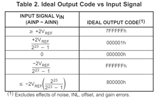
    Please note that the ADS1222 uses a binary two's complement coding scheme (see below), so 0x00000h = 0d (decimal), while 0xFFFFFFh = -1d (decimal). Therefore, the values you are seeing are 0 and -1.

    Did you see any values at the ADC output other than 0xFFFFFF or 0x00000?

    Also, we might need to see the communication coming from the ADC, so hopefully you have access to a logic analyzer

    -Bryan

  • Hi Bryan,

    I am sharing schematic over private message.

    I dont see other values than 0x00 and 0xFF.

  • Hi Tony,

    What voltages are you seeing at the input of the ADC? Can you measure them with a DMM and report back? Please also do this for the reference voltage

    Why do you have a voltage divider on your DOUT pin?

    -Bryan

  • Hi Bryan,

    The voltage measured at VREFP is 3.0V.

    Voltage at AINP1 pin is 0V and other than 0V when pressure applied.

    The MUX pin is reset to 0

    Thanks,

    Thi

  • Hi Tony,

    Can you be more specific than "other than 0V"? What is the actual voltage? And when you start the ADC conversion, what is the ADC data when this nonzero voltage is applied?

    Can you probe the ADC DOUT pin (the ADC pin, not the controller pin) to verify that the ADC is sending out either all 1s (FFFFFF) or all 0s (000000)? Perhaps there is an issue with the actual communication path

    Also, why do you have a resistor divider on your DOUT pin?

    Have you tried replacing the ADC to see if the issue goes away?

    Are you seeing this issue on your other boards, or just this one board?

    -Bryan

  • Hello Bryan,

    I could figure out the issue. Its due to the frequence inputs to CLK pin.

    Finally, I could see meaning values of raw ADC but I am still concerned about it.

    The behavior is that when power up, the data received is 0x7FFFFF.

    When the pressure applied, the value decreased. The more pressure increase, the more value decreased received.

    Is that proper behavior?

    And one more issue is that when I made the ratchet go the other way, the ADC value received didn't change.

    It looks like the MUX selection and self-calibration doesn't affect on those issues, doesn't it ? 

    Thanks,

    Tony

  • Hi Tony,

    0x7FFFFF is the maximum positive code, which would make sense at powerup. Maybe the reference voltage hasn't fully powered up yet, so it is basically 0V. You also have a very large gain (>300x) on your input. So any small signal, offset, etc., will likely give a positive full-scale reading i.e. 0x7FFFFF. I would suggest waiting until the system is fully powered and settled before actually taking any data. The data will be meaningless prior to this settled point

    • What are the input signals you are trying to measure?
    • What is your VDD voltage?
    • What is the value of the resistor network at the input (RN1 and RN2)?

    -Bryan

  • Hi Bryan,

    WRT the issue of 0x7FFFFF, I only started reading after a couple of minutes. I think it is long enough for the system get fully powered.

    The second issue is not answered: When I made the ratchet go the other way, the ADC value received didn't change. What should be the problem ?

    Below are some points you just wanted to know

    • What are the input signals you are trying to measure? We are developing a POC for digital ratchet which allows monitoring torque.
    • What is your VDD voltage? VDD is 2.5V
    • What is the value of the resistor network at the input (RN1 and RN2): RN1 - 20kΩ, RN2 - 20kΩ

    Thanks

  • Hi Tony,

    Let me clarify my question: what is the output signal magnitude from the sensor? 10mV? 1mV? In other words, what is the voltage range you are applying to the amplifier?

    The second issue is not answered: When I made the ratchet go the other way, the ADC value received didn't change. What should be the problem ?

    What value is the ADC output code at this point? Is it also 0x7FFFFF?

    -Bryan

  • What value is the ADC output code at this point? Is it also 0x7FFFFF?

    Yes, The value of 0x7FFFFF remains the same

    what is the output signal magnitude from the sensor?

    It is 3mV

    Thanks

  • Hi Tony,

    Can you try not dividing down the reference voltage to 1.25V, and instead just use VDD (2.5V) as the reference voltage. Let me know if this allows you to get code changes.

    -Bryan

  • Hello Bryan,

    I just tried to remove the resistors so that the ref voltage became 2.5V but the issue persists.

    Actually, the design with ADS1222 part are working fine with the other MCU.

    Can you please have a look at resistor networks RN3 (100kOm) RN4 (200kOm). Are they properly designed?

  • Hi Tony,

    Can you please have a look at resistor networks RN3 (100kOm) RN4 (200kOm). Are they properly designed?

    What is the point of these resistor networks? It looks like these are connected to GPIO pins, that switch in/out the 6Mohm resistor on the (+) pin on each amplifier - is that correct? That looks like it would apply a resistor divider to the (+) pin on the amplifier, making the bias point just a little bit lower voltage compared to normal. Why do you have this?

    Actually, the design with ADS1222 part are working fine with the other MCU.

    So you have one MCU that is working correctly, and one MCU that is not? Are these different controllers, or you just have one board that is working and one that is not?

    -Bryan

  • Why do you have this?

    The purpose is for adding offset into amplifier.

    With 4pins for 2 resistor networks, 4 pairs of value would be available to select.

    So you have one MCU that is working correctly, and one MCU that is not? Are these different controllers, or you just have one board that is working and one that is not?

    It is working fine with STM32 board

    The issue is now happening on new board with RL78 MCU with the same design for peripheral parts.

    I am wondering about power up sequence for the sensor or pins configuration.

    Tony

  • Hi Tony,

    Then to be honest, this does not sound like an ADC issue. Maybe there is some timing difference between the old controller and the new controller?

    But if the ADC circuit works with one MCU and not with another, then you have an MCU issue. I don't think I will be able to offer further assistance since this is not a problem with the ADS1222

    -Bryan

  • Hi Bryan,

    Thank you for continuous support.

    After trying to output different levels on GPIO for resistor networks, I could receive ADC value about +- 22900 (X) at no load. The value varied X-- for one way  and X++ for the other way. Is this proper behavior.

    And could I consider X value as "zero ADC" then during measuring, If Y value received, real ADC value would be (Y-X).

    Thanks,

    Tony      

  • Hi Tony,

    I could receive ADC value about +- 22900 (X) at no load. The value varied X-- for one way  and X++ for the other way. Is this proper behavior.

    This feels like a lot of variation, but it's probably because you have such a large gain in your system (>300x). So any small change is going to be amplified a lot

    And could I consider X value as "zero ADC" then during measuring, If Y value received, real ADC value would be (Y-X).

    Effectively, yes. This is your offset. You might also perform a gain calibration at the higher end of signal range. You can read more about load cell / scale calibration in section 5.5 of Guide to Bridge Measurements document: https://www.ti.com/lit/an/sbaa532a/sbaa532a.pdf?ts=1720023143007

    -Bryan