


Tool/software:
Hello,
We are facing a problem with the DAC39J84 seemingly not recognizing K-symbols from the TI JESD IP core.
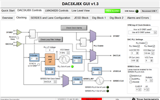
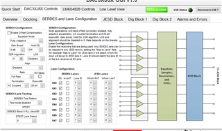
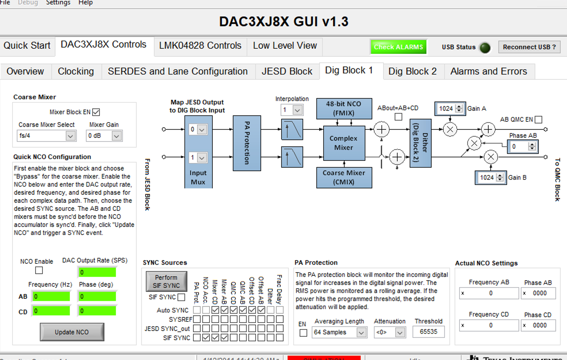
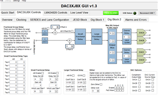
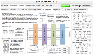
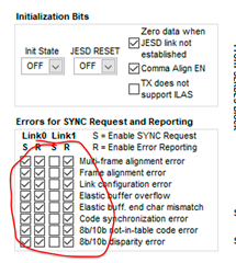
Here is what we see in the TI GUI:
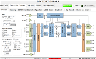
Here is the value of all the registers of the DAC:
In the Vivado logic analyzer we see the following:
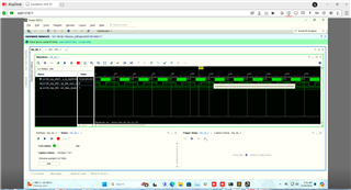
SYNC is "blinking" (From low to high and back) - it all looks like the receiver (DAC) did not recognize the bcbcbcbcbc string (K-symbol)
Our SYSREF is 3906250Hz.The DAC reference clock is 1GHz. Our SYSREF is pulsing in continuous mode since our clock chip provide it in "unlimited mode".
Here are the SYSREFs in the Vivado HW analyzer:
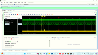
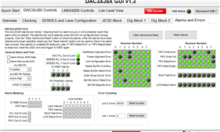
We "played" with this checkbox. When all boxes are checked - SYNC is pulsing from 1 to 0 and back. It appears like the DAC detected a lot of errors and according to this window, is trying to SYNC repeatedly.
Our desired lane rate is 10Gbps (our ADCs on the same board are operating well at this speed)
Our write sequence is the following:
static dac39j84_spi_t dac39j84_init_regs[] =
{
//This do Software Reset and 4 wires
{0x02, {0x20, 0x03}}, // [15:14] dac_bitwidth = 00
// [13]zer_inv = 1
// [12]shorttest_en = 0
// [7]sif4_en = 0
// [6]mixer_en = 0
// [5]mixer_gain = 0
// [4]nco_en = 0
// [1]twos = 1
// [0]sif_rst(wsc) = 1
//Set 4 wires after softreset
{0x02, {0x20, 0xC2}}, // [15:14] dac_bitwidth = 00 (16 bit)
// [13]zer_inv = 1 (Zero the data from the JESD block when the link is not established)
// [12]shorttest_en = 0
// [7]sif4_en = 1 (SIF interface becomes a 4 pin interface)
// [6]mixer_en = 1 Mixer enabled
// [5]mixer_gain = 0
// [4]nco_en = 0
// [1]twos = 1
// [0]sif_rst(wsc) = 0
// This is part for coarse mixer
/*****************************************************************
{0x0D, {0x44, 0x00}}, // Set FS/4 for mixer
{0x2F, {0x00, 0x04}}, // [14] titest_dieid_read_ena
// [0] sifdac_ena
{0x30, {0x00, 0x00}}, // sifdac
{0x1F, {0x99, 0x80}}, // [15:12-11:8] syncsel_mixer(ab-cd)
// [7:4] syncsel_nco [1] sif_sync
{0x1F, {0x99, 0x82}}, // [15:12-11:8] syncsel_mixer(ab-cd)
// [7:4] syncsel_nco [1] sif_sync
{0x1F, {0x99, 0x80}}, // [15:12-11:8] syncsel_mixer(ab-cd)
// [7:4] syncsel_nco [1] sif_sync
**************************************************************************/
// Set TXENABLE to LOW
{0x03, {0xF3, 0x80}}, // [15:12] coarse_dac = 1111
// [7] fif_error_zd_en = 1
// [1] sif_txen = 0
// Programm the DAC PLL Settings
{0x1A, {0x00, 0x20}}, // [8] vbgr_slp = 0
// [7] biasopamp_slp = 0
// [6] tsense_slp = 0
// [5] pll_slp = 1 // We will not use PLL
// [4] clkrecv_slp = 0
// [3:0] dac(a:d)_slp = 000
{0x1B, {0x01, 0x00}}, // [15] extref_en = 0
// [14:12] tdest_lane = 000
// [11:8] dtest = 0001
// [5:0] atest = 00000
{0x31, {0x70, 0x30}}, // [15:13] lockdet_adj = 000
// [12] rst = 1 // We will not use PLL
// [11] ndivsync_ena = 0
// [10] en = 0 // We will not use PLL
// [9:8] cp = 00
// [7:3] n = 00000
// [2:0] lfvolt(RO) = 000
/*
//Let it be default values
{0x32, {0x00, 0x00}}, // [15:8] m = 00000000
// [7:4] p = 0000
{0x33, {0x01, 0x80}}, // [15] vcosel = 0
// [14:9] vco = 000000
// [8:7] vcoitune = 10
// [6:2] cp_adj = 00000
*/
// Program the SERDES settings
// With this settings we get clock from DAC inputs directly, and divide it by 2x, so we get 500Mhz (1Ghz/2=500Mhz) as the refclock for serdes PLL
{0x3B, {0x08, 0x00}}, // [15] serdes_clk_sel = 1 (1 = PLL, 0 = Pins) NOTE: Documentation LIES
// [14:11] serdes_refclk_div = 0001 (Divide by 2x ?????)
{0x3C, {0x80, 0x28}}, // [15] endivclk = 1 (enables output of a divide-by-5 of PLL clock)
// [12:11] LB = 0
// [10] SleepPLL = 0
// [9] Vrange = 0
// [8:1] MPY = 00010100 (5x, It means that we get 500Mhz, mpy it by 5 and get 2500Mhz (2.5Ghz x 4 = 10000))
{0x3D, {0x00, 0x08}}, // [14:12] testpatt =
// [7] enoc =
// [6] eqhld =
// [5:3] eq =
// [2:0] cdr =
{0x3E, {0x01, 0x08}}, // [15:13] los = 000
// [10:8] term = 001 Common point set to 0.7V. This configuration is for AC coupled systems.
// The transmitter has no effect on the receiver common mode, which is set to optimize the input sensitivity of the receiver
// [6:5] rate = 00 Full rate. Four data samples taken per SerDes PLL output clock cycle
// [4:2] buswidth = 010 (20bit)
// [1] sleeprx = 0
// [0] resered = 0
// Program the SERDES lane settings
/*
// Let it be the default values
{0x3F, {0x00, 0x00}}, // [7:0] INVPAIR = 00000000 (All Lanes are not inverted)
{0x46, {0x00, 0x44}}, // [15:11] lid0 =
// [10:6] lid1 =
// [5:1] lid2 =
{0x47, {0x19, 0x0A}}, // [15:11] lid3 =
// [10:6] lid4 =
// [5:1] lid5 =
{0x48, {0x31, 0xC3}}, // [15:11] lid6 = 00110
// [10:6] lid7 = 00111
// [3:1] = 00
// subclassv = 001
// [0] jesdv = 1
{0x49, {0x00, 0x00}}, // link_assign = 0, default
*/
{0x4A, {0xFF, 0x1E}}, // [15:8] lane_ena = 11111111 (ENABLED ALL 8 LANES)
// [7:6] jesd_test_seq = 00
// [5] dual = 0
// [4:1] init_state = 1111 (PUSH IN JESD in INIT STATE)
// [0] jesd_reset_n = 0 (JESD IN RESET)
/*
//Let it be the default values
{0x5F, {0x01, 0x23}}, // [14:12] octetpath_sel(0)
// [10:8] octetpath_sel(1)
// [6:4] octetpath_sel(2)
// [2:0] octetpath_sel(3)
{0x60, {0x45, 0x67}}, // [14:12] octetpath_sel(4)
// [10:8] octetpath_sel(5)
// [6:4] octetpath_sel(6)
// [2:0] octetpath_sel(7)
*/
{0x25, {0x20, 0x00}}, // [15:13] clkjesd_div = 001 //interpolation*L/M = 1*8/4 = 2
{0x24, {0x00, 0x10}}, // [6:4] cdrvser_sysref_mode
{0x00, {0x00, 0x08}}, // [15] qmc_offset_ab_en= 0
// [14] qmc_offset_cd_en= 0
// [13] qmc_corr_ab_en = 0
// [12] qmc_corr_cd)_en = 0
// [11:8] interp = 0
// [7] az_txen = 0
// [6] outsum_ena = 0
// [5] az_jesd_en = 0
// [4] ao_en = 0
// [3] ao_pol = 1
// [2] pap_en = 0
// [1] inv_sinc_ab_ena = 0
// [0] inv_sinc_cd_ena = 0
// Program the JESD settings
{0x03, {0xF0, 0x80}}, // [15:12] coarse_dac = 1111
// [7] fif_error_zd_en = 1
// [1] sif_txen = 0
{0x4B, {0x1F, 0x00}}, // [12:8] rbd_m1
// [7:0] f_m1
{0x4C, {0x1F, 0x07}}, // [12:8] k_m1 = 11111 (K = 32)
// [4:0] l_m1 = 0111 (All Lanes used by JESD)
{0x4D, {0x03, 0x00}}, // [15:8] m_m1 = 3 (This is the number of converters per link)
// [4:0] s_m1 = 0 (This is the number of converter samples per frame)
{0x4E, {0x0F, 0x4F}}, // [12:8] nprime_m1 = 0xF (This is the number of adjusted bits per sample)
// [6] hd = 1 (Turns on/off High Density mode for the JESD. When asserted samples are split across 0 lanes)
// [5] scramble = 0 (Turns on/off the scrambler function in the JESD block)
// [4:0] n_m1 = 0xF (This is the number of bits per sample. NOTE: 15 is the only valid value)
{0x4F, {0x1C, 0x41}}, // [15:8] match_data = 00011100
// [7] match_specific = 0
// [6] match_ctrl = 1
// [5] no_lane_sync = 0
// [0] jesd_commaalign_ena = 1
{0x51, {0x00, 0x01}}, // [15:8] did_link0
// [7:0] sync_request_ena_link0 = 0x0F
{0x54, {0x00, 0x00}}, // [15:8] did_link1
// [7:0] sync_request_ena_link1 = 0x00
/*
// Let it be default values
{0x50, {0x00, 0x00}}, // [15:12] adjcnt_link0
// [11] adjdir_link0
// [10:7] bid_link0
// [6:2] cf_link0
// [1:0] cs_link0
{0x52, {0x00, 0xFF}}, // [9] disable_err_report_link0
// [8] phadj_link0
// [7:0] error_ena_link0
{0x53, {0x00, 0x00}}, // [15:12] adjcnt_link1
// [11] adjdir_link1
// [10:7] bid_link1
// [6:2] cf_link1
// [1:0] cs_link1
{0x55, {0x00, 0xFF}}, // [9] disable_err_report_link1
// [8] phadj_link1
// [7:0] error_ena_link1
*/
{0x5C, {0x11, 0x11}}, // [7] err_cnt_clr_link1
// [6:4] sysref_mode_link1
// [3] err_cnt_clr_link0
// [2:0] sysref_mode_link0
{0x61, {0x00, 0x01}}, // [15] syncn_pol = 0
// [11:8] syncncd_sel = 0
// [7:4] syncnab_sel = 0
// [3:0] syncn_sel = 001
/*
// Let it be default values
{0x1E, {0x11, 0x11}}, // [15:12-11:8] syncsel_qmoffset(ab-cd)
// [7:4-3:0] syncsel_qmccorr(ab-cd)
{0x1F, {0x11, 0x40}}, // [15:12-11:8] syncsel_mixer(ab-cd)
// [7:4] syncsel_nco [1] sif_sync
{0x20, {0x88, 0x88}}, // [15:12] syncsel_dither
// [7:4] syncsel_pap
// [3:0] syncsel_fir5a
*/
{0x6C, {0x00, 0x00}}, // [15:12] alarm_sysref_err = 0
// [11:8] alarm_pap = 0
// [3:2] alarm_wr(0:1)_pll = 0
// [0] alarm_from_pll = 0
// This shall start JEST INIT (SYNC PIN TO LOW and wait for K-symbols)
{0x4A, {0xFF, 0x01}}, // [15:8] lane_ena = 11111111
// [7:6] jesd_test_seq = 00
// [5] dual = 0
// [4:1] init_state = 0000 (PULL OUT JESD of INIT STATE)
// [0] jesd_reset_n = 1 (JESD OUT OF RESET)
// Set TXENABLE to HIGH
{0x03, {0xF3, 0x81}}, // [15:12] coarse_dac = 1111
// [7] fif_error_zd_en = 1
// [1] sif_txen = 1
};
We believe we have done these settings correctly according to the datasheet. However, since the DAC seems to not recognize the K-symbols, it is not passing the CGS stage.
We look forward to your support
Thanks,
Ryan
