Other Parts Discussed in Thread: LMK04828
Dear all,
I'm struggling with the configuration of the DAC39J84.
I do not see any outputs from the DAC due to errors on the lanes. Even if I'm able to perform the NCO test and the PRBS test mode is successful. I kindly ask you if you can check the configuration of the DAC.
This is my configuration:
- FMC120 from abaco DAC39J84 and LMK04828
- Trenz board with TE0808 with 9EG.
On the FPGA side I'm usign the IP xilinx JESD204b (PG066) and IP JESD204 PHY (PG198).
I'm communicating with the DAC trough a I2C to SPI bridge.
Here is how the LMK is connected to the DAC and to FPGA and what the expected frequencies are :
internal reference of the Board at 100 Mhz CLK2in input of LMK
DCLK0 → 1000 Mhz DAC clock
DCLK2 → 250 Mhz clock open in the design for debug
DCLK4 → 1000 Mhz ADC A clock
DCLK6 → 1000 Mhz ADC B clock
DCLK8 → 250 Mhz clock connected to the GTH Lines
DCLK10 → 250 Mhz clock connected to the GTH Lines
The configuration register are set as in the file lmk04828.txt.
LMK0482 configuration
0x0000   0x0010
0x0002   0x0000
0x0003   0x0006
0x0004   0x00d0
0x0005   0x005b
0x0006   0x0020
0x000c   0x0051
0x000d   0x0004
0x0100   0x0063
0x0101   0x0022
0x0102   0x0055
0x0103   0x0005
0x0104   0x0062
0x0105   0x0000
0x0106   0x0032
0x0107   0x0055
0x0108   0x006c
0x0109   0x0022
0x010a   0x0055
0x010b   0x0005
0x010c   0x0062
0x010d   0x0000
0x010e   0x0032
0x010f   0x0011
0x0110   0x0063
0x0111   0x0022
0x0112   0x0055
0x0113   0x0005
0x0114   0x0062
0x0115   0x0000
0x0116   0x0032
0x0117   0x0055
0x0118   0x0063
0x0119   0x0022
0x011a   0x0055
0x011b   0x0005
0x011c   0x0062
0x011d   0x0000
0x011e   0x0032
0x011f   0x0057
0x0120   0x006c
0x0121   0x0022
0x0122   0x0055
0x0123   0x0005
0x0124   0x0062
0x0125   0x0000
0x0126   0x0037
0x0127   0x0001
0x0128   0x006c
0x0129   0x0022
0x012a   0x0055
0x012b   0x0005
0x012c   0x0062
0x012d   0x0000
0x012e   0x0037
0x012f   0x0001
0x0130   0x0060
0x0131   0x0022
0x0132   0x0055
0x0133   0x0005
0x0134   0x0042
0x0135   0x0000
0x0136   0x00ff
0x0137   0x0000
0x0138   0x0020
0x0139   0x0002
0x013a   0x0006
0x013b   0x0000
0x013c   0x0000
0x013d   0x0008
0x013e   0x0002
0x013f   0x0000
0x0140   0x0000
0x0141   0x0000
0x0142   0x0000
0x0143   0x0013
0x0144   0x00ff
0x0145   0x007f
0x0146   0x0000
0x0147   0x002c
0x0148   0x0033
0x0149   0x0000
0x014a   0x0000
0x014b   0x0020
0x014c   0x00ff
0x014d   0x0000
0x014e   0x0000
0x014f   0x007f
0x0150   0x0000
0x0151   0x0002
0x0152   0x0000
0x0153   0x0000
0x0154   0x0078
0x0155   0x0000
0x0156   0x0000
0x0157   0x0000
0x0158   0x000a
0x0159   0x0000
0x015a   0x0032
0x015b   0x00df
0x015c   0x0020
0x015d   0x0000
0x015e   0x0000
0x015f   0x000b
0x0160   0x0000
0x0161   0x0004
0x0162   0x00d0
0x0163   0x0000
0x0164   0x0000
0x0165   0x0004
0x0166   0x0000
0x0167   0x0000
0x0168   0x0004
0x0169   0x0049
0x016a   0x0000
0x016b   0x0020
0x016c   0x0000
0x016d   0x0000
0x016e   0x0013
0x0171   0x00aa
0x0172   0x0002
0x0173   0x0000
0x0174   0x0000
0x017c   0x0015
0x017d   0x0033
0x0182   0x0002
0x0183   0x0002
0x0184   0x00a0
0x0185   0x0000
0x0188   0x0000
0x1ffd   0x0000
0x1ffe   0x0000
0x1fff   0x0000
As it is possible to see form the configuration I'm programming the SYS REF as a gapped pulse.
For the DAC these are the main parameters:
L = 8
M = 4
F = 1
S = 1
HD = 1
Fdac = 1000 MHz
DACPLL enabled, VCO L-BAND P=4, M=2, N=2
JESD CLOCK DIVIDER 2
SERDES: 10 Gbps, Full Rate, PLL @ 2.5GHz, serdes_refclk_div=2, MPY =0b10100
Here the programming sequence
|
Operation Read/Write |
Address |
Value |
Notes |
|
HW DAC_RESET |
(after applying this reset the DAC sif registers have the default values, so this hw reset is working) |
||
|
Write |
0x02 |
0x0082 |
|
|
Read |
0x7F |
0x800a |
From data sheet versionid=0x1 from this register read is 0x2 |
|
write |
0x1A |
0x0 |
|
|
write |
0x0 |
0x18 |
|
|
write |
0x25 |
0x2000 |
JESDCLK_DIV |
|
write |
0x31 |
0x6C08 |
|
|
write |
0x32 |
0x120 |
|
|
write |
0x33 |
0xAF40 |
|
|
write |
0x3B |
0x8800 |
|
|
write |
0x3C |
0x828 |
|
|
write |
0x3D |
0x8E |
|
|
write |
0x3E |
0x108 |
|
|
write |
0x3F |
0x0 |
|
|
write |
0x46 |
0x44 |
|
|
write |
0x47 |
0x190A |
|
|
write |
0x48 |
0x31C3 |
|
|
write |
0x49 |
0x0 |
|
|
write |
0x04 |
0xFF |
Alarm MASK |
|
write |
0x05 |
0xC0F2 |
Alarm MASK |
|
write |
0x06 |
0xFF00 |
Alarm MASK |
|
write |
0x24 |
0x10 |
SYSREFMODE_for_clkdvr |
|
write |
0x1E |
0x2222 |
set_SYSREF_for_DSP |
|
write |
0x1F |
0x2220 |
set_SYSREF_for_DSP |
|
write |
0x20 |
0x2022 |
set_SYSREF_for_DSP |
|
write |
0x23 |
0x2022 |
set_SYSREF_for_DSP |
|
write |
0x5C |
0x1111 |
SYSREFMODE_for_JESD |
|
write |
0x34 |
0x80 |
SYNC set the LVDS format |
|
write |
0x4B |
0x1F00 |
Buffer=32 Frames = 1, Octets per frame = 1 |
|
write |
0x4C |
0x1F07 |
K=32,L=8 |
|
write |
0x4D |
0x0300 |
M = 3 S = 1 |
|
write |
0x4E |
0xF4F |
SCR=0, High Density, N=16 N'=16 |
|
write |
0x4F |
0x1CC1 |
|
|
write |
0x51 |
0xFF |
|
|
write |
0x52 |
0xFF |
|
|
write |
0x54 |
0xFF |
|
|
write |
0x55 |
0xFF |
|
|
write |
0x5F |
0x123 |
|
|
write |
0x60 |
0x4567 |
|
|
write |
0x01 |
0x0000 |
|
|
write |
0x03 |
0xA300 |
|
|
write |
0x61 |
0x211 |
|
|
DAC_TX_EN |
|||
|
write |
0x4A |
0xFF1E |
|
|
write |
0x4A |
0xFF1F |
|
|
write |
0x4A |
0xFF01 |
|
|
Enable 1 PULSE on LMK04824 |
|||
|
Clearing the config100-config107 (writing all 1 and then all zeros) |
|||
|
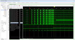
the lanes status registers config100-config107 gives 0x400 |
|||
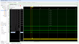
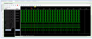
So we have a 'code synchronization error' and nothing from the DAC outputs.
After the DAC programming sequence I can see that the SYNC signal after toggling it stays high.
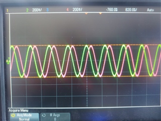
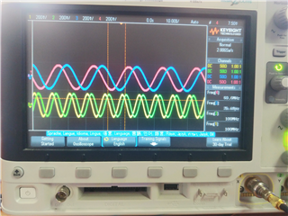
To see if I can obtain the output from the DAC and the SYSREF from the LMK, I tried to perform the NCO TEST and once I configured the output level from the SIF, the MIXER frequencies and send a SYSREF pulse I can obtain the sinusoids that I expect.
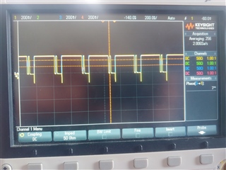
The other test I performed is the PRBS test by sending a PRBS sequence from FPGA and configuring the DAC lane by expecting the same PRBS or a different one.
The Alarm Pin goes high when the DAC expecting a diffent sequence, and it stays low when the PRBS sequence is correct. So from these test it looks like the SERDES link doesn't have any problems.
I also perform the link layer tests(about these tests I'm not completly sure about the programming sequence):
ILA test from conf100-107 I obtain always 0x400
K28.5 test: conf100-107 I obtain always 0x0
D21.5 test : conf100-107 I obatin always 0x0
So apparently, the code synchronization error seems to be the problem.
Do you have any suggestions on how I can solve this problem?
Thanks for the attention