Tool/software:
Hi,
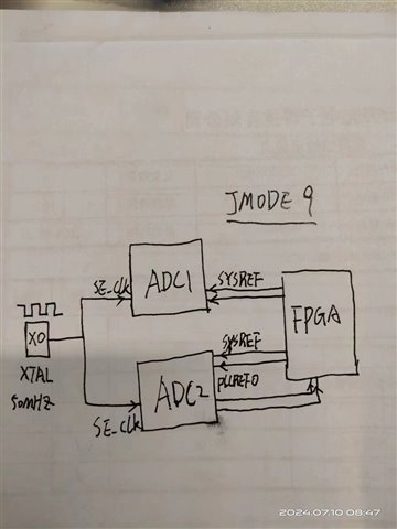
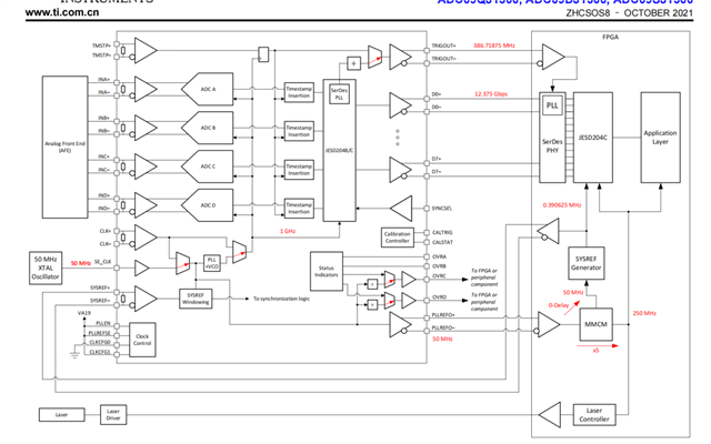
The project is based on the jesd204b protocol to implement two ad09qj1300 data transmissions, with an external 50MHz crystal oscillator as the clock input, AD sampling rate=1G, JMODE=10, and subclass 1 mode.
The refclk of jesd204b phy uses the trigout adjoint clock of ADC at 195.3125 MHz (R/32), the core_clk is the ADC's 50 MHz reference clock, which is multiplied to 156.25 MHz (R/40), and the sysref clock (195.3125 Khz) is obtained by dividing the reference clock. During the link establishment process, there are the following issues:
1. Our board (with two ADC chips on the same board) came back for power on testing and found that there are two default ADC power consumption situations. Later, the program read and found that the S-PLL of the ADC on the board with low power consumption was not locked. After normal program configuration, all ADCs were normal again. What is the reason for the different default ADC states.
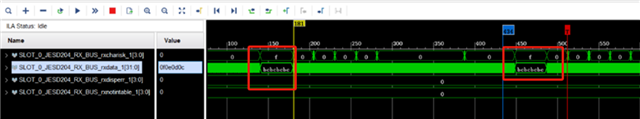
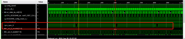
2. When 0x207='h02 (K28.5) and 0x205='h04 (ramp), sync successfully raises. However, when modifying 0x205='h05 (short transmission), sync loses lock and exhibits periodic changes. The jesd204b register shows an unexpected K-code received, as shown in the following figure:
After modifying 0x207='h01 (K28.1), in different testing modes, sync successfully and stably raised the level. Why do K28.5 and K28.1 cause different phenomena? Why is there such a difference?
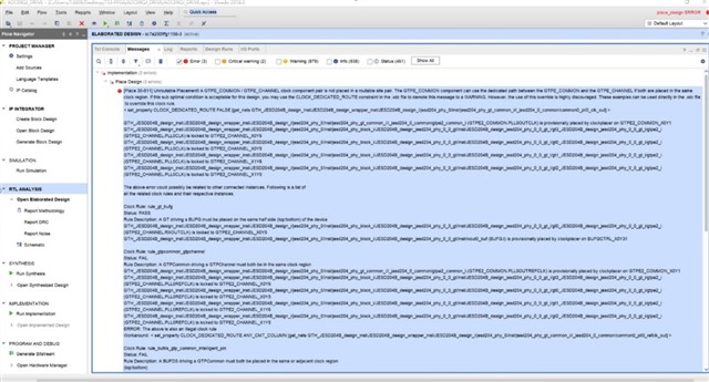
3. What should be noted when allocating pins for GTP dedicated clock and data pins in FPGA? Due to the multiplexing of clocks in two banks, must data pins in the same bank be assigned to the same bank? Please provide detailed information that the following errors may occur when the allocation is inappropriate:
Thanks!