This thread has been locked.

If you have a related question, please click the "Ask a related question" button in the top right corner. The newly created question will be automatically linked to this question.

ADC12D1800: LVDS

Part Number: ADC12D1800

Tool/software:

Hi,

I want to interface the LVDS Differential O/Ps of this ADC to Virtex Ultrascale Plus FPGA with HP IO bank.

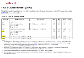
Below is from ADC datasheet. 

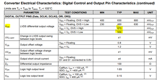
Below is Virtex Ultrascale FPGA HP IO bank characteristics (Link) : table 19

1. What is the Common mode voltage of the differential ADC Outputs for AC and DC coupling? Will it match the FPGA receiver characteristics highlighted above?

2. Based on FPGA datasheet, Differential mode spec of FPGA is max 600mV. Is this an issue to integrate with the ADC outputs?
We have previous used Virtex6 in older design with same ADC and didn't see any issue on this. But since we are going for a new FPGA, want to be sure of this. 

Thanks.

  • Hi Nandini,

    The LVDS common mode voltage is by default 0.8V. If you see the description for pin B1 (Vbg) then you will find if this pin is tied to logic high (ie connected to V_A) then the LVDS common mode level changes to 1.2V.

    The output swing is adjustable and programmed by register 0x0 bit 13. If this bit is high, then outputs will swing by 670mVpp. If this bit is programmed low, then the outputs will swing by 500mVpp. The power on reset value for this register bit is 1 so when the device is powered on, you will temporarily be receiving data on the LVDS interface of 670mVpp. This will continue until you write this bit as 0, at which point the interface will switch to 500mVpp mode. You will have to check the Virtex US+ maximum section as mentioned in the footnote #3 to see if this 670mVpp will damage the device or not.

    Thanks, Chase

  • Hi Chase,

    From the same table, VIDIFF max value is 600mV.

    There are no other values mentioned for maximum limit for VDIFF in the datasheet: Link

    Is this a problem?

  • Nandini,

    If you see footnote 3 it says you can lower common mode to account for higher swing. I’ve mentioned what the ADC can do. I don’t know what the fpga can do. I do not support Xilinx parts and am not going to go look through their datasheet for exact details.

    Thanks, Chase