This thread has been locked.

If you have a related question, please click the "Ask a related question" button in the top right corner. The newly created question will be automatically linked to this question.

TLA2518: Clocks and conversion timing

Part Number: TLA2518

Tool/software:

Hello team,

My customer has several questions regarding clock and conversion timing.
Would it be possible to answer questions below?

1. When customer is not using averaging filter, can they ignore OSC_SEL and CLK_DIV[3:0] setting? It seems like they are only used for averaging module.

2. What is the benefit or usecase of Manual Mode over On-the-Fly mode? It seems like On the fly mode is better because there is no latency for channel selection.

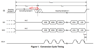
3. What is the Figure 1 (Conversion Cycle Timing) implying?
   Does it mean that user has to pull CS HIGH to start conversion and pull CS LOW manually to start sample acquisition?
   OR is it going to start the Acquisition automatically, when conversion is done. Will it pull the CS by the ADC?
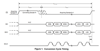
   

4. tACQ is 400ns (MIN) from the datasheet.

When 50MHz of SPI is used, the 12 clock would be 240ns, so it seems impossible to achieve 400ns of tACQ.
Is this true?
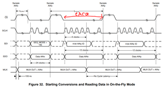
5. What are Quiet acquisition time and quiet conversion time? I couldn't find any explaination from the datasheet.

Best Regards,
Kei Kuwahara

  • Hi Kei,

    1. Yes, while the averaging is disabled, the OSC_SEL and CLK_DIV fields can be kept as default.

    2. In short, in some customer applications, the 2 conversion cycle delay from channel selection with SDI to channel data on SDO isn't much of a concern. Manual mode will usually be chosen if many conversions are being read from the same channel in succession. To switch channels, one will write to the MANUAL_CHID[3:0] field. To some customers, this register write to switch channels is preferable to always including the channel address for the next conversion on SDI. On-the-fly mode will provide less latency from when you want a channel to switch and that channel's data comes out though.

    3. Yes, CS needs to be held high by the controller for a minimum of t_conv, then brought low to initiate the next conversion cycle. CS will not be controlled by the ADC, and it won't be done automatically. 

    4. Yes, you are correct, but the maximum sampling rate of the ADC is rated only up to 1MSPS. For conversion at 1MSPS, a clock greater than 13.5 MHz should be used (this is inclusive of conversion and acquisition time). A higher clock frequency can be used for digital read/writes of the device registers, and GPIO operations. SCLK should not be higher than 30 MHz during conversion of an analog input, as this would violate the 400ns acquisition time minimum required. 

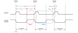
    5. Quiet acquisition time is explained best in this tech note. It is listed in the figure you included under question 3 as "t_QUIET". Quiet conversion time is also known as quiet aperture time. Any noise during td_cnvcap can negatively affect the result of the ongoing conversion whereas any noise during tqt_acq can negatively affect the acquisition of the subsequent sample. See below as to where they are within the timing diagram. Here, CONVST is instead CS. 

    Regards,
    Joel

  • Hello Joel-san,

    Thank you for your detailed explaination!

    My customer has additional questions.

    3. Yes, CS needs to be held high by the controller for a minimum of t_conv, then brought low to initiate the next conversion cycle. CS will not be controlled by the ADC, and it won't be done automatically. 

    So customer can set the t_conv by how long they are going to pull CS HIGH right? Is is going to improve the accuracy of the measurement, when taking t_conv much longer than maximum conversion time of 600ns (from datasheet)?

    4. Yes, you are correct, but the maximum sampling rate of the ADC is rated only up to 1MSPS. For conversion at 1MSPS, a clock greater than 13.5 MHz should be used (this is inclusive of conversion and acquisition time). A higher clock frequency can be used for digital read/writes of the device registers, and GPIO operations. SCLK should not be higher than 30 MHz during conversion of an analog input, as this would violate the 400ns acquisition time minimum required. 

    I thought t_ACQ is decided by how long the user is going to pull the CS LOW, or is t_ACQ decided by the SCLK frequency (1/f * 12 clocks)?

    5. Quiet acquisition time is explained best in this tech note. It is listed in the figure you included under question 3 as "t_QUIET". Quiet conversion time is also known as quiet aperture time. Any noise during td_cnvcap can negatively affect the result of the ongoing conversion whereas any noise during tqt_acq can negatively affect the acquisition of the subsequent sample. See below as to where they are within the timing diagram. Here, CONVST is instead CS. 

    I couldn't find quiet time for conversion on the datasheet. Can I assume it to be 10ns before the CS is pulled low after conversion?

    Best Regards,
    Kei Kuwahara

  • Hi Kei-san,

    t_CONV is the time it takes for the ADC to convert an input on its sample capacitor after acquisition of the input signal, so this generally stays fixed regardless of sampling rate or how long CS is held high. Holding CS higher for longer won't improve accuracy, as the input signal voltage has already been sampled at the sample capacitor, and won't change. 

    What will change with SCLK and sampling rate is t_acq. As you said, for this device, it will take 12 SCLK cycles, plus a little bit of overhead. t_acq will actually make the determination on how much time the input signal has to settle within a desired accuracy.

    Yes, t_QUIET is not found in the datasheet, but it is equal to the 10ns minimum in the quiet acquisition and quiet conversion times given. I will speak with systems on whether this can be clarified in the next datasheet revision to indicate they are the same. 

    Regards,
    Joel