This thread has been locked.

If you have a related question, please click the "Ask a related question" button in the top right corner. The newly created question will be automatically linked to this question.

ADS131M08: I actually want to know the detailed mechanism between the behavior of the DRDY pin and the 2 'FIFO inside the device.

Part Number: ADS131M08

Tool/software:

Recently I ran into some issues while debugging ADS131M08. Some features of ADS131M08 are not well understood.

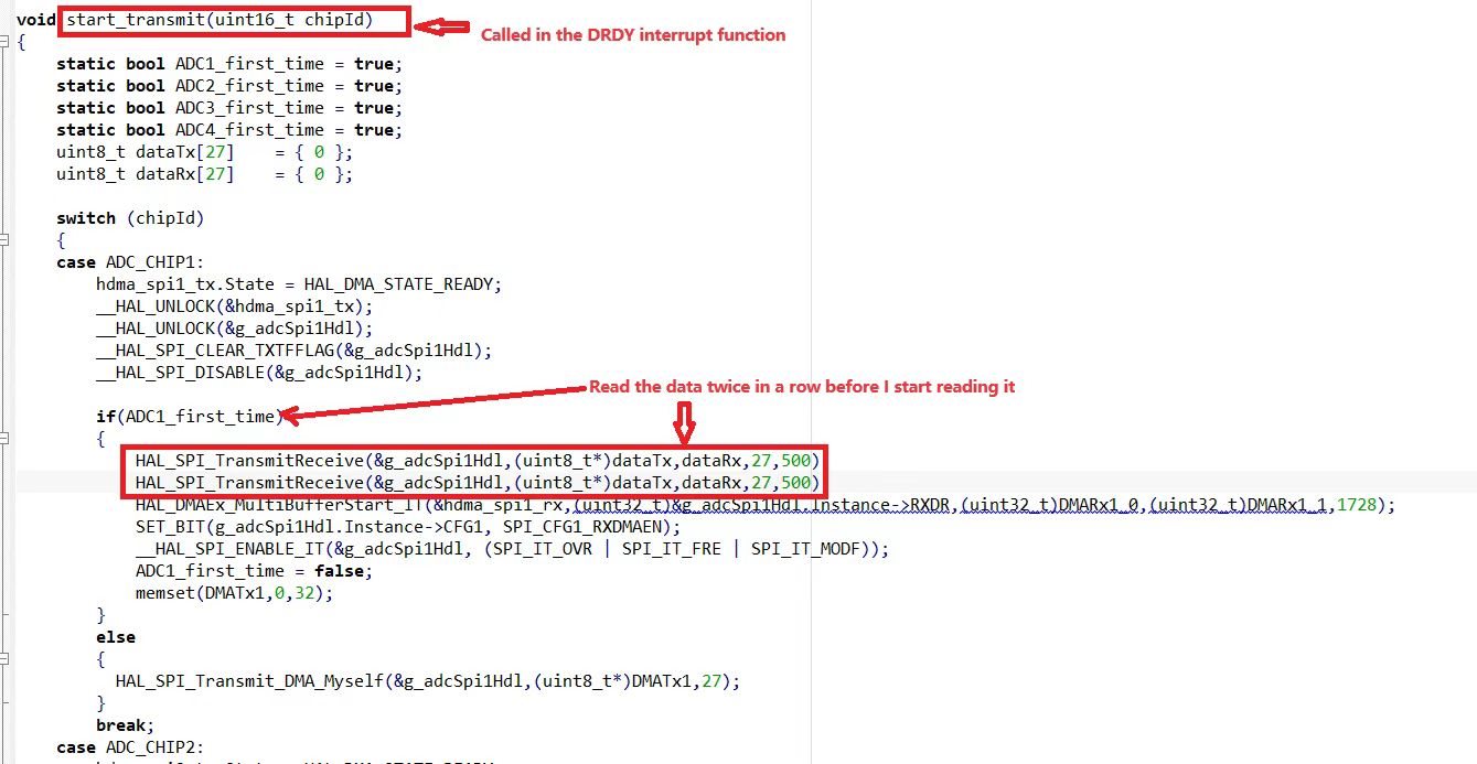
My project is to use STM32H7 as micro control, SPI+DMA way to read data.

Following the instructions in the data sheet, two consecutive frames are read before DMA is enabled. Why read two frames in a row first? I didn't do what the manual said, so DRDY no longer behaves at the rate I set. For example, I set it to 8KSPS, but the actual performance rate is less than 1K.

I actually want to know the detailed mechanism between the behavior of the DRDY pin and the 2 'FIFO inside the device. ”

  • Hello,

    The behavior of the DRDY pin and the output data depend on how you retrieve the data from the ADC, are you reading the conversion data by monitoring the /DRDY signal or DRDY bit in the STATUS register or waiting for a certain amount of time? would you please share your timing plots for SPI bus including /DRDY signal?

    BR,

    Dale

  • I read the ADC data by detecting the behavior of the DRDY pin. That is, whenever a DRDY interrupt occurs, I will enable SPI Tx DMA to send NULL commands, while SPI Rx DMA is also enabled. Below I will share the timing waveforms of SPI CLK and DRDY lines under normal and abnormal conditions. It can be seen that the DRDY frequency in the normal case is 8k and the DRDY frequency in the abnormal case is 249Hz

  • Hi,

    Thank you for providing these information. Were you able to read or write internal registers correctly?

    I noticed that your question, "two consecutive frames are read before DMA is enabled. Why read two frames in a row first? I didn't do what the manual said, so DRDY no longer behaves at the rate I set." Can you please clarify "read two frames in a row first"? Were you talking about the following timing from the datasheet?

    Also, please clarify "two consecutive frames are read before DMA is enabled".

    BR,

    Dale

  • I read the value of status register (0x01) and it is 1280. The ADC conversion value I read is unstable and feels inaccurate. Below is my code.

  • Hi user4637774,

    The default data of the STATUS register should be 0500h. The wrong data you got indicates your timing is incorrect. Let's correct your timing first by reading internal registers.

    Below is a timing example to read Gain register (04h address) in the first frame and the response 0x0E0E register data which was previous programmed is shown in the 2nd frame, can you please capture a similar timing with your circuit board and software? you can read the default data from some registers (e.g. CLCOK or CFG register) after the ADC is powered up. Your schematic will be helpful to debug too.

    BR,

    Dale