This thread has been locked.

If you have a related question, please click the "Ask a related question" button in the top right corner. The newly created question will be automatically linked to this question.

DAC81402: Questions for Bipolar Output Mode (-5V to 5V) of DAC81402

Part Number: DAC81402

Tool/software:

Hello, This is Kwonjoon Lee.

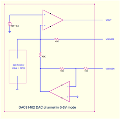
We would like to ask some questions about Figure 8-1 in the datasheet of DAC81402.
(www.ti.com/.../dac81402)

(Questions)

1. Should we apply 5V and -5V to AVDD and AVSS, respectively, for generation of bipolar DAC output? (corresponding to -5V to 5V)

2. Should we connect the REFGND and SENSEN pins to Ground (0V) in order to obtain bipolar DAC output? (corresponding to -5V to 5V)

3. Could you provide more detailed circuit for the “Resistor Gain Network”?

    According to Table 8-1 in the datasheet of DAC81402, register setting for bipolar DAC output (-5V to 5V) results in the GAIN factor corresponding to 4.

    However, we cannot understand how the analog circuit including the “Resistor Gain Network” (in lower-right corner of Figure 8-1) sets the GAIN factor to 4.

Best regards,
Kwonjoon Lee

  • Hi Kwonjoon,

    1) Yes, you would need to supply at least +5V to AVDD and -5V to AVSS to generate the bipolar DAC output of +/-5V. 

    2) Yes, these two pins should be grounded.

    3) I will ask a designer for more information on the resistor gain network.

    Thanks,
    Erin

  • Hi Kwonjoon,
     
    Diagram is correct only and Resistor Gain Network will be set in such a way that the total looking in resistance from inverting terminal to GND will be ~40k/3.
    Let me know if need any more details.
     
    Regards,
    Sanjay

  • Hi Sanjay,

    Thank you very much for your previous answer.


    (Additional Question)

    In the case that
    1) we use "unipolar output mode (0V-5V)", and
    2) we connect "SENSEN" pin to ground (0V),

    Should the total resistance (at the node of inverting terminal of the output buffer amp)
    seen looking into the circuits including "Resistor Gain Network" be ~40kOhm?
    (in this observation and calculation, we would like to neglect the resistor, 40kOhm connected to the "SENSEP" pin)


    Best regards,
    Kwonjoon Lee

  • Hi Kwonjoon,

    Below is the equivalent circuit diagram for the 0 - 5V output range of DAC81402. As you can see from the diagram Resistor Gain Network will be "open".


    Hope this helps.

    Thanks,
    Sanjay

  • Hi Sanjay,

    I really appreciate your kind answers.
    This is the last question.

    (Last question)

    1.If we use unipolar output mode (0V-5V) in the Figure 9-1 of the datasheet, 
       sourcing or sinking (DC) current of the output buffer amplifier of the DAC81402 will be lower than 100uA
       because the non-inverting amplifier input of the motor control module (in the Figure 9-1) is high resistance node, and
       internal feedback resistance around the output buffer amplifier is only 40kOhm.

       In this situation, I would like to ask if the AVDD supply voltage of the DAC81402 can be lower to 5.5V.
       (According to the Figure 7-31 of the datasheet, headroom corresponding to only ~0.5V is required for the sourcing DC current corresponding to ~5mA)


    Best regards,
    Kwonjoon Lee

  • Hi Kwonjoon,
      
    Thank you for the kind words, I am here to answer as many as questions you, that's not a problem for me.
     
    Yes, you are right. You can reduce your supply AVDD voltage below 5.5V as DAC81402 output amplifier is suppling only 0.1mA (much less than the 5mA ) 
      
    Hope I was able to clarify your doubt.
      
    Thanks,
    Sanjay