This thread has been locked.

If you have a related question, please click the "Ask a related question" button in the top right corner. The newly created question will be automatically linked to this question.

ADS114S08: Technical Questions + Design Review

Part Number: ADS114S08

Tool/software:

Hi team, I have some questions regarding the ADS114S08:

Filter design (based on this app note):

1. In example 3.1, I want to confirm my understanding of the filter design / requirements. The anti-aliasing is handled by the internal decimation filter with a cutoff around 3.5 Hz, so your external filter is used for attenuating external noise on the RTD lines. Where did the ~250 Hz frequency cutoff to achieve this come from?

2. As the part multiplexes through multiple inputs (ie IDAC chopping, measuring REFP0, REFN0), the effective sample rate will decrease because you're not measuring every input at an interval of 20Hz, how do I be sure that there's effective anti-aliasing in this case? 

3. How are idle tones accounted for in this design / what parameters on the data sheet reflect this performance, as this will be likely measuring a near-DC voltage?

4. Many of the references I've seen for this part show the REFN pin have a filter where one end is grounded. Is there any advantage to this versus just grounding the pin directly and using a single ended filter for REFP?

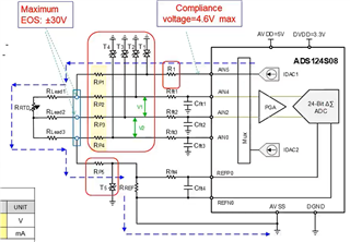
Input protection (based on this app note):

1. Is there a reason the input / output nets are protected twice, one for each pin? I assume it's to maintain a kelvin style connection right to the connector. Would there be a significant downside to using one resistor and diode near the connector and using a kelvin connection to there?

General:

1. Is there any advantage to using an external clock with one or multiple parts? 

Thanks in advance for taking the time to answer these questions. Please let me know if we could set up a design review as well.

Best,

Nick

  • Hi Nick Robinson,

    Answers to your questions:

    In example 3.1, I want to confirm my understanding of the filter design / requirements. The anti-aliasing is handled by the internal decimation filter with a cutoff around 3.5 Hz, so your external filter is used for attenuating external noise on the RTD lines. Where did the ~250 Hz frequency cutoff to achieve this come from?

    You can review this video to better help your understanding with respect to anti-aliasing and digital filters: https://www.ti.com/video/series/precision-labs/ti-precision-labs-analog-to-digital-converters-adcs.html?videoId=6196470400001

    This video might help as well: https://www.ti.com/video/5422293803001

    As the part multiplexes through multiple inputs (ie IDAC chopping, measuring REFP0, REFN0), the effective sample rate will decrease because you're not measuring every input at an interval of 20Hz, how do I be sure that there's effective anti-aliasing in this case? 

    See the previous answer

    How are idle tones accounted for in this design / what parameters on the data sheet reflect this performance, as this will be likely measuring a near-DC voltage?

    Idle tones generally are visible in the output spectrum using shorted inputs. When applying a relatively small DC input, or an AC signal, the idle tones tend to disappear. Also, note that idle tones are not visible on every device, and I have not heard of customers seeing idle tones with the ADS114S08.

    Many of the references I've seen for this part show the REFN pin have a filter where one end is grounded. Is there any advantage to this versus just grounding the pin directly and using a single ended filter for REFP?

    It is always best practice to place the filter cap on REFP/REFN directly across the pins and as close to the device as possible.

    Is there a reason the input / output nets are protected twice, one for each pin? I assume it's to maintain a kelvin style connection right to the connector. Would there be a significant downside to using one resistor and diode near the connector and using a kelvin connection to there?

    This video (and the subsequent videos in this series) helps explain why the system was designed this way: https://www.ti.com/video/series/precision-labs/ti-precision-labs-analog-to-digital-converters-adcs.html?videoId=6303631504001

    Is there any advantage to using an external clock with one or multiple parts?

    If you want to synchronize multiple devices, or if the internal clock accuracy is insufficient for your application, you might consider an external clock

    -Bryan

  • These look like really great resources, thanks for sharing. I'll take some time to familiarize myself with these and make a new post if there are any outstanding questions at that point.

  • Hi again, I took some time to look through some of these resources. I still have some outstanding questions, especially around the protection circuitry:

    1. The operation of a TVS diode is described, but I don't understand why a TVS is chosen for this application vs a Zener. This EOS is a DC voltage instead of a transient, wouldn't a Zener be specified for DC operation so that it's easier to specify and select a part? Or is it so the design could potentially protect against transient voltages as well, even if they are not specified by this design note.

    2. I'm still not entirely sure why each pin is protected separately instead of each leg of the RTD (5 pins including IDACs vs 3 circuits for RTD). At first, I thought it was for the kelvin connection, and then I thought it might be because the current limits through the internal ESD diodes are specified per pin, but the current drawn from one pin at a voltage is the same either way. When I simulate the circuit I see the same performance in both configurations.

    Thanks for taking the time to review my questions,

    Nick

  • Hi Nick Robinson,

    Answers to your questions:

    The operation of a TVS diode is described, but I don't understand why a TVS is chosen for this application vs a Zener. This EOS is a DC voltage instead of a transient, wouldn't a Zener be specified for DC operation so that it's easier to specify and select a part? Or is it so the design could potentially protect against transient voltages as well, even if they are not specified by this design note.

    Your last comment is correct, the design was intended for transients as well as EOS, which is why TVS were used

    I'm still not entirely sure why each pin is protected separately instead of each leg of the RTD (5 pins including IDACs vs 3 circuits for RTD). At first, I thought it was for the kelvin connection, and then I thought it might be because the current limits through the internal ESD diodes are specified per pin, but the current drawn from one pin at a voltage is the same either way. When I simulate the circuit I see the same performance in both configurations.

    The current into each pin must be limited to <10mA. So in the image below for example, AIN5 and REFP0 would not be protected if you only applied the protection to the IDAC pins.

    And you cannot connect the IDAC before the resistors (e.g. between Rflt1 and AIN4), because then the IDAC current flows through Rflt1 and RP2 and would be measured by AIN4, which would cause an error (a similar circumstance occurs where REFP connects to AIN0, this connection must be made after the protection circuitry)

    -Bryan