This thread has been locked.

If you have a related question, please click the "Ask a related question" button in the top right corner. The newly created question will be automatically linked to this question.

ADC124S021: cpol, cpha

Part Number: ADC124S021

Tool/software:

Dear Community,

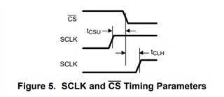
While analyzing the serial timing diagram in the datasheet, I’m unable to determine the values of CPOL and CPHA. Could you please clarify what they are? Additionally, on page 5 (note 2), it states: "Clock may be either high or low when CS is asserted as long as setup and hold times tCSU and tCLH are strictly observed." Does this mean I can use two different values for CPOL?

Thank you.

  • Hi Luigi,

    Data is clocked out on DOUT on the falling edge of SCLK. This means that data will be valid for the controller to sample on the rising edge of SCLK. There are two valid possibilities for this device; SPI Mode 3 (CPOL = 1, CPHA = 1), and SPI Mode 0 (CPOL = 0, CPHA = 0).

    SPI Mode 3 is shown by the first SCLK below, where SCLK goes high before CS falls. In this case, the first bit of DOUT is clocked out on the first falling edge of SCLK after CS goes low, and will be sampled on the following rising edge of SCLK.

    SPI Mode 0 is shown by the second SCLK below. Here, SCLK is held low before the falling edge of SCLK, and it is here that the falling edge of CS clocks out the first bit of DOUT, which would then be valid to read by the controller on the next rising edge.  

    The decision on which to use will be up to you, but I imagine SPI Mode 3 will be easier to implement and ease the timing requirements.

    Regards,
    Joel

  • Hi Joel,

    I noticed that you wrote SPI Mode 3 and SPI Mode 0 with the same parameters (CPOL = 1, CPHA = 1). Typically, SPI Mode 0 has CPOL = 0, CPHA = 0. Could you please clarify if there was an error in your description?

    Regards, 

    Luigi

  • Hi Luigi,

    Yes, this was a mistake. I have fixed it now.

    Regards,
    Joel