This thread has been locked.

If you have a related question, please click the "Ask a related question" button in the top right corner. The newly created question will be automatically linked to this question.

ADC12QJ1600EVM: ADC12QJ1600EVM

Part Number: ADC12QJ1600EVM

Tool/software:

hello,

I under stand that the LMK can accept on clkin1 in pin  in distribution mode up to 3Ghz.

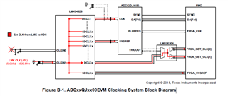
I wish to design a system according the below diagram (Figure B-1. ADCxxQJxx00EVM Clocking System Block Diagram FROM SLAU808.pdf)

- Input clock to clkin1 of the LMK is 1Ghz.

- DCLK out to the ADC clk in also 1Ghz = sample rate 

- ADC in JMODE8 = 4 lanes/ 12bit/64/66 = lane rate of 12.375Gbps 

- According to ADC Data Sheet  Trig Out will be 386.71875MHz (Lane rate/32 or could be /64) used optionally to FPGA GBT clock.

- Given all the above I need to know what is the frequency LMK generates on the output going to FPGA GBT clock?

Regards,

Giora

  • Hello,

    Any answer for the above?

    Regards,

    Giora

  • Hello Giora,

    The design you are showing has the lmk distributing clocks to both the ADC and FPGA. The LMK has many different use cases and can be configured many different ways. On this board it is only used in its simplest mode which is distribution mode. Which means the clock that is input is either bypass to the output (meaning that what you put on the input you get at the output) or through a divider. So for example if you want to sample at 640 MHz, you could apply a single 640 MHz tone at the input of the LMK and then the clock path to the ADC would bypass the divder. For the fpga clocks these could then be passed through a divider to be divided down to the correct frequency depending on the JMODE of the ADC which is selected.

    In short the LMK has many different ways it can be configured and it is really up to you how you would like to use it exactly.

    Best,

    Eric

  • Hello Eric,

    According to your answer can I input 1Ghz and output for example 386.71875MHz (for JMODE 8 12b 66/64)

    For my understanding in distribution mode it is not possible.

    Regards,

    Giora

  • Hello Giora,

    The ADC has three clock requirements

    1) Sample Clock (in your case it is 1 GHz)

    2) FPGA reference Clock, this is a reference provided to the FPGA transceivers so they can lock on to the correct line rate of the data coming out of the ADC, think about this as a reference to a PLL on the FPGA.

    3) JESD Core Clock, this is the clock the JESD system will run off of.

    In most designs the JESD Core clock needs to be either a ratio of Linerate/66 for 64b66b or Linerate/80 for 8b10b, (this also assumes the datawidth inside the JESD core is 64 bits) In this case given a sample clock of 1 GHz the Linerate will be 12.375 Gbps for JMODE 8 which means the Core Clock needs to be 187.5 MHz.

    For the XCVR clock many different clocks are valid as long as they are integer divisors of the line rate, so for simplicity sake we typically make the XCVR_CLOCK = CORE_CLOCK. So for this mode both clocks will run at 187.5 MHz.

    What you are seeing in the reference design in the datasheet is that the FPGA Clocks are being generated by the ADC chip itself, which comes from the trigout pins of the ADC. The output clock only has available divider values of 32, 64 and 128 which are non standard values as per what I have explained earlier. So in order for this mode to work you will have to adapt your firmware to accept these clock divider values. Again in your case of 1 1 GHz clock the clock values would be 388.71875 MHz, 193.359375 MHz and 96.6796875 MHz. In this operation of the ADC evm the LMK is not used as all the clocks can come from the ADC.

    So can you confirm what exact use case you want to use of the ADC?

    For your question "According to your answer can I input 1Ghz and output for example 386.71875MHz (for JMODE 8 12b 66/64)

    For my understanding in distribution mode it is not possible."  This is correct it would require the lmk to have a fractional divider which is why on the ADC board we have multiple different clocking options to support different modes. However, there is a solution given that you want to use the LMK and not the ADC trigout pins the FPGA Clock frequency needs to be 187.5 MHz actually and not 386.71875 MHz as I have explained above. Given this we need to find the lowest common multiple of both 1 GHz (Sample Clock) and 187.5 MHz (Ref Clock) which comes out to be 3000 MHz or 3 GHz. This means we can apply a 3 GHz tone to the LMK input and use the dividers on the LMK to get the correct clock frequencies. For instance to generate a 1 GHz sample clock we would have to use a divider value of 3 because 3000/3 = 1000. And for the reference clock we would have to use a divider value of 16 as 3000/16=187.5 MHz. So as you can see it would still be possible for the LMK to generate all the clocks given only one input tone.

    Best,

    Eric

  • Eric,

    Thanks for the clarification.

    Giora